vidivici.world
Junior Member level 3
I'm plotting a PCB file based on a reference design (so no schematic files) and encounter a problem.
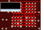
One chip with FBGA pinout gets the pad inside out through via. Now I want to connect this pad to another place, but just cannot select the via connecting to it and change its net.
It seems that all vias in this FBGA pinout have been bonded together and you just cannot select one single via. Is there some way to break it and select just one of these vias?