Continue to Site

Welcome to EDAboard.com

Welcome to our site! EDAboard.com is an international Electronics Discussion Forum focused on EDA software, circuits, schematics, books, theory, papers, asic, pld, 8051, DSP, Network, RF, Analog Design, PCB, Service Manuals... and a whole lot more! To participate you need to register. Registration is free. Click here to register now.

measure gain margin and phase margin

Status
Not open for further replies.

thanhtri_pc

Junior Member level 2
Joined
Apr 18, 2010
Messages
22
Helped
0
Reputation
0
Reaction score
0
Trophy points
1,281
Location
Vietnam
Activity points
1,458
hi all,
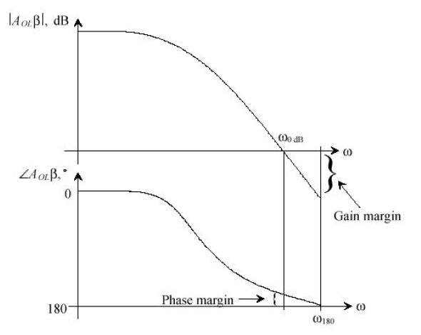
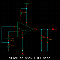
I want to determine the gain and pharse margin of the Op-amp (open-loop only). So I draw the schematic as attachment.

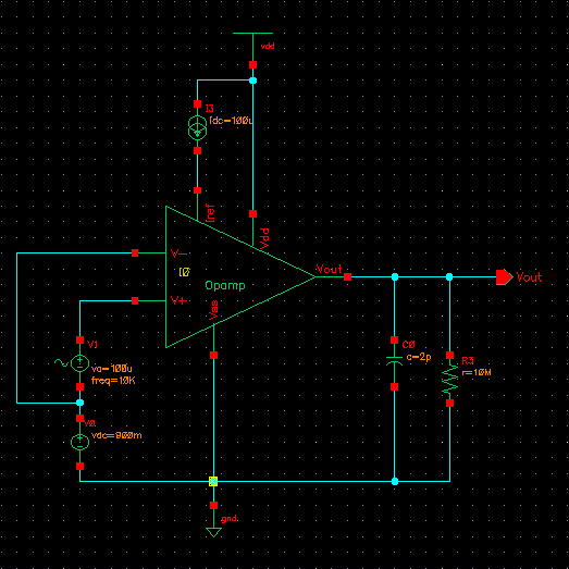
The input is Vsin signal and I run AC analysis (using Spectre simulaor). After simulating, I realize that with different magnitude of Vsin, I got different values of gain/pharse margin. I would like to ask how to choose the magnitude value of Vsin to get valid gain/pharse margin?
Many helps are welcome!
 

Ac analysis - if performed correctly - is independent on the ac amplitude (small signal analysis).
Check and correct the dc operating point of the opamp (use dual supply).
 
Last edited:

I think that you shouldn't use Vsin, instead of this put a Vdc and evaluate 1V for the ac voltage attribute inside the symbol. If there is Vac at you project it will be useful also.

try this and I think that your problem will be solved
 

Yes, masa_2010 is right. Your simulation setup does not show an ac analysis (opposite to your own statement in the first posting).
 

Hi all,
You can see my op-amp use single supply power (vdd=1.8V, Vss = 0). So, in schematic, I use an Vdc to create offset voltage in oder to bias all of transistor of op-amp operate in saturation region. After that I use Vsin (connect serial with Vdc). I also run AC analysis, but I have a problem: I got different gain/pharse margin with different magnitude of Vsin.
 

20log(Vout) is used to plot the graph. So when u are reading the gain from the graph, it is correct only if the magnitude of Vsin is 1V. Else u need to reduce the gain by 20logVsin to get the correct value. Please make sure that u are doing this when u are varying the magnitude of Vsin.
 

Hi all,
You can see my op-amp use single supply power (vdd=1.8V, Vss = 0). So, in schematic, I use an Vdc to create offset voltage in oder to bias all of transistor of op-amp operate in saturation region. After that I use Vsin (connect serial with Vdc). I also run AC analysis, but I have a problem: I got different gain/pharse margin with different magnitude of Vsin.

I think, your simulation setup is "problematic". That means, it may work for some opamps but it may fail for some other types.
The problem area is the operating point that certainly is NOT in the middle of the available operating range due to missing negative feedback. Let the simulator display the dc output voltage - and you will see what I mean.
Your setup with a fixed offset (Vdd/2) is identical to a dual supply setup with both inputs dc grounded.
This works only for an ideal model without any offset properties.
I would suggest to use a setup with negative feedback. Then, you can apply one of the classical methods for open loop simulations. These methods have been discussed several times in this forum and elsewhere.
 

Another thing, how can you test the phase margin and gain margin if there is no feedback at the circuit ?
Generally, the stability issue appears only at closed loop systems. If your system is open loop, this mean that it will be always stable.
 

Yes masa_2010, in principle you are right. However, it is common practice - for example, in data sheets - to give a phase margin also for opamps without feedback. In this case, the specified margin applies for the worst case which is unity gain feedback.
For all other feedback values the margin is larger.
 

Hi LvW,

Can you please tell why the phase margin is worst in the case of unity gain buffer?

Thanks,
VIjay
 

In my opinion, I don't think PM for unity gain buffer is the worst case. This comment is only correct when the feedback is only pure resistor divider. The unity gain buffer will have the biggest loop gain (the feedback factor is 1). For other pure resistor divider case, the feedback factor will be less than 1, so it results in a smaller loop gain. If pole and zero is no change, it leads to higher bandwidth and more drop in phase. Therefore, phase margin with unity gain feedback is the lowest. But if the feedback is more than pure resistor divider, it is hard to say. For example, one more cap is connected between feedback node to ground, it might lead to worse phase margin than that of unity gain buffer.
 

It's easy to make mistakes when measuring phase and gain margin. Are you measuring as shown in image attached ?


Status
Not open for further replies.

Part and Inventory Search

Welcome to EDABoard.com

Sponsor

Back
Top