ella1923
Member level 1
gain boosted folded cascode amplifier
hi everyone!
i am designing a gain boosted cascode folded opamp and i have done with my
main amplifier of 40dB and 300MHz. right now, i am doing the gain boosted ota.
the paper that i have read says that the input and ouput of the gain boosted
opamp are to be set, marked as red in the figure.
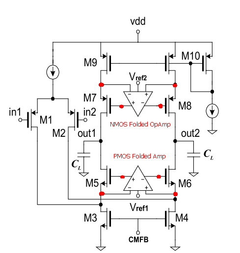
what i did in my gain boosted ota design was,
vin+,vin- is equal to Vds of (m3,m4) and Vds of (m9,m10);
vout+,vout- of pmos folded opamp is equal to vin+/vin- plus vt(m5,m6)
plus vds(m5,m6) while for nmos folded opamp is equal to vin+/vin- plus
plus vt(m7, m8) plus vds(m5,m6)
Is this correct? Because when I tried to connect the gain boosted amplifier to
the main amplifier, some transistors were linear and cutoff. By the way, i have
set Vref1 and Vref2 nearly equal to the output of the gain boosted opamp which
is also the gate voltage of m5,m6,m7 and m8.
If you have any idea regarding what was wrong with the design, please enlighten
me. My target design is >85dB gain and >250MHz UGB.
thank you very much.
regards,
ella
hi everyone!
i am designing a gain boosted cascode folded opamp and i have done with my
main amplifier of 40dB and 300MHz. right now, i am doing the gain boosted ota.
the paper that i have read says that the input and ouput of the gain boosted
opamp are to be set, marked as red in the figure.
what i did in my gain boosted ota design was,
vin+,vin- is equal to Vds of (m3,m4) and Vds of (m9,m10);
vout+,vout- of pmos folded opamp is equal to vin+/vin- plus vt(m5,m6)
plus vds(m5,m6) while for nmos folded opamp is equal to vin+/vin- plus
plus vt(m7, m8) plus vds(m5,m6)
Is this correct? Because when I tried to connect the gain boosted amplifier to
the main amplifier, some transistors were linear and cutoff. By the way, i have
set Vref1 and Vref2 nearly equal to the output of the gain boosted opamp which
is also the gate voltage of m5,m6,m7 and m8.
If you have any idea regarding what was wrong with the design, please enlighten
me. My target design is >85dB gain and >250MHz UGB.
thank you very much.
regards,
ella