Continue to Site

Welcome to EDAboard.com

Welcome to our site! EDAboard.com is an international Electronics Discussion Forum focused on EDA software, circuits, schematics, books, theory, papers, asic, pld, 8051, DSP, Network, RF, Analog Design, PCB, Service Manuals... and a whole lot more! To participate you need to register. Registration is free. Click here to register now.

Input match of a CS-LNA considering the bondwire and pad

Status
Not open for further replies.

lsfeng

Junior Member level 1
Joined
Oct 5, 2007
Messages
19
Helped
0
Reputation
0
Reaction score
0
Trophy points
1,281
Activity points
1,429
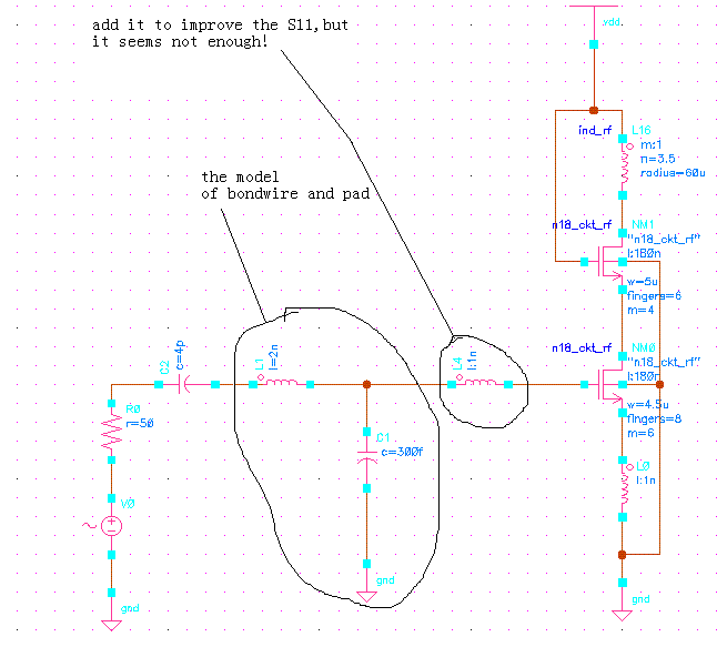
now I am designing a common source LNA ,and the S11 is very bad(-7,8dB),I want to make it better by improve the
input match network.Considering the effect of bondwire and pad of input signal,the quetion seems more difficult to me,the schematic is as follows ,how can I make an input match network to achieve both a good S11 and NF at the same time ,thank you!

ps: the book " microwave egineer" is usefull for RF designing?


the source degenration inductor used to increasee the real part of the input impedance , while the gate inductor used to eleimtae the imaginary capacitive part , but u have another section u need to know how this section affect the input imedance of ur circuit , then re design the Ls and Lg to give u the best result

sure if u read about matching circuits in microwave books will be very usefull

khouly
 

thank u very much for ur advise ,i think i should learn more theory about matching firstly,
any how it becomes more complicated consideing the effect of bondwire and pad of input, output,gnd and vdd,and my circuit is working on 3-5GHz, it's really awful things!!!
 

sure the multi Ghz RFIC , these effects of bondwires and pads must be taken into account ,

u need to check how the bondwire intuctance will affect the impedance

khouly
 

Status
Not open for further replies.

Part and Inventory Search

Welcome to EDABoard.com

Sponsor

Back
Top