stamford
Newbie level 6
Hi all,
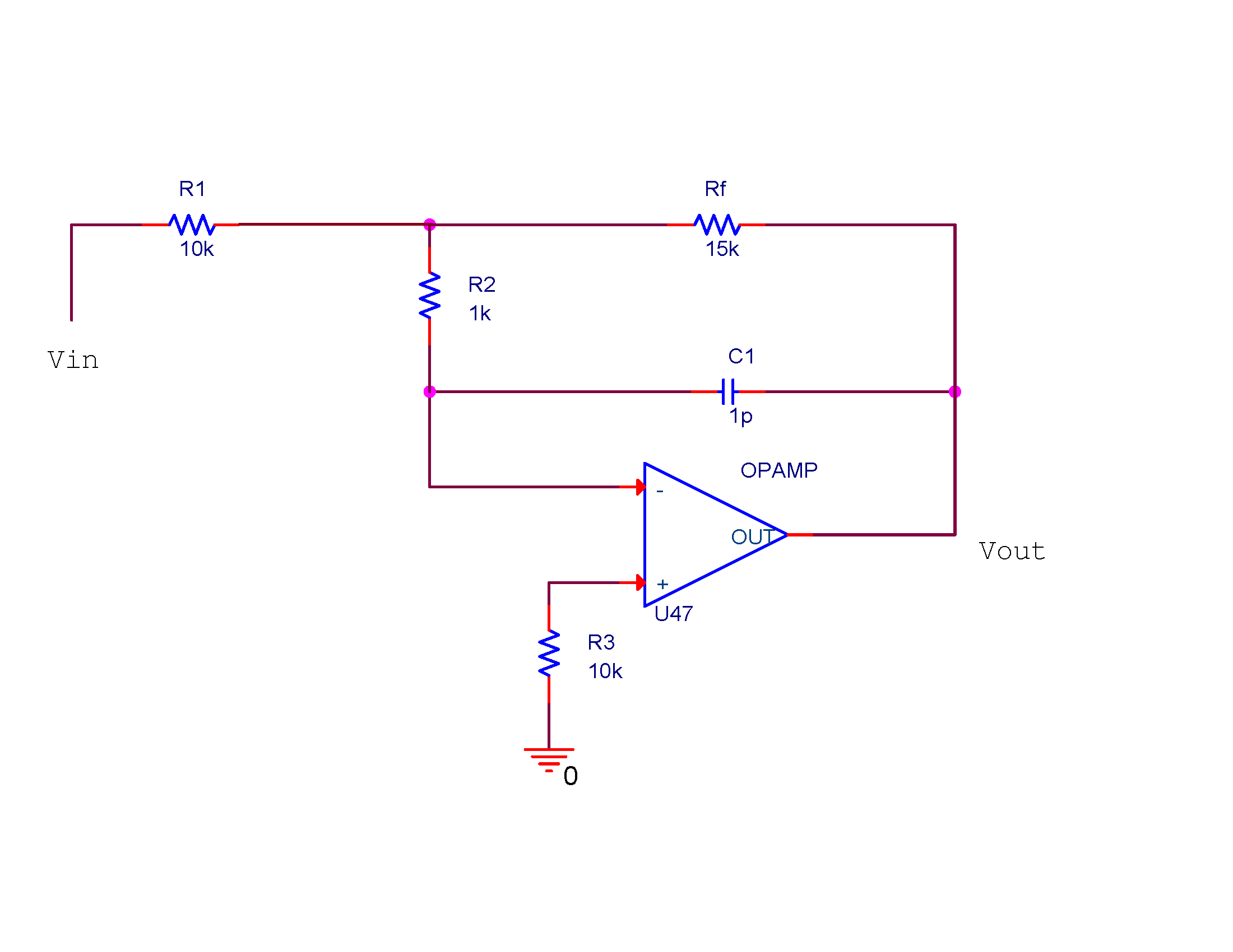
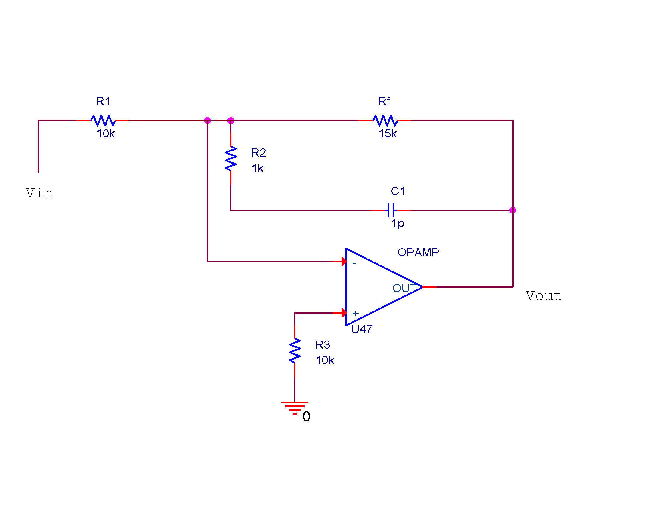
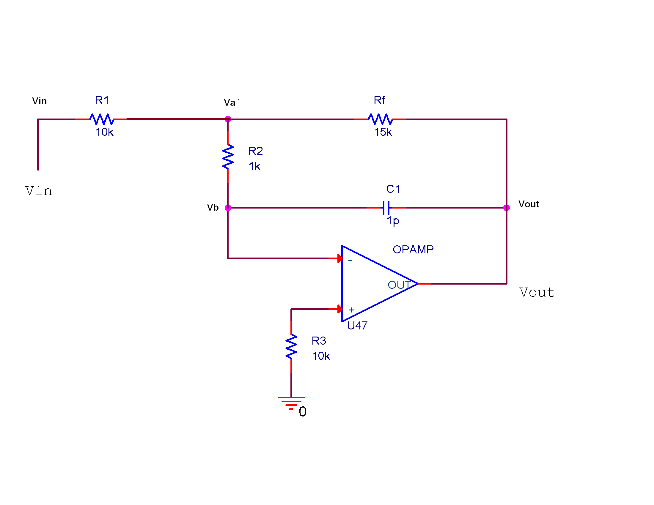
I came across a simple inverting amplifier circuit. It has a capacitor in parallel to the feedback amplifier.
I can tell the circuit functions as an inverting amplifer with a gain of 15 and that no (negligible ??) current flows through the capacitor and the 1k resistor.
Can anyone please tell me whats the function of the 1pF capacitor and the 1K resistor ? .