Continue to Site

Welcome to EDAboard.com

Welcome to our site! EDAboard.com is an international Electronics Discussion Forum focused on EDA software, circuits, schematics, books, theory, papers, asic, pld, 8051, DSP, Network, RF, Analog Design, PCB, Service Manuals... and a whole lot more! To participate you need to register. Registration is free. Click here to register now.

Altera Quartus: How to write and read the data into FIFO ?

Status
Not open for further replies.

AbinayaSivam

Member level 1
Joined
Jul 27, 2017
Messages
38
Helped
0
Reputation
0
Reaction score
0
Trophy points
6
Activity points
345
Hello,

I am running 32-bit counter in Quartus. I have used the PIO to read the data but i am facing the problem, data is not in sequence in which PIO receiving the data slowly from FPGA. So, i think FIFO is best to store and read the data in NIOS.

I am new to the altera, please anyone share the FIFO example design or else guide me in FIFO design.

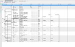
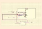
I have attached the Screenshot of the design in which i have used PIO.
https://forums.intel.com/s/question/0D50P000041tK2g/how-to-print-counter-output-in-nios-console-?s1oid=00DU0000000YT3c&OpenCommentForEdit=1&s1nid=0DB0P000000U1Hq&emkind=chatterCommentNotification&s1uid=0050P000008Ifj2&emtm=1536152201613&fromEmail=1&s1ext=0
 

Attachments

  • Nios.JPG
    Nios.JPG
    98.2 KB · Views: 227

What if the Nios is always slower (or faster) at reading the data compared to you supplying it with new data?
Simply using a FIFO won't suffice in such a case.
You'll also have to monitor the FIFOs flags...

If the purpose of your project is simply to see things working - you don't have to design your own FIFO. Just generate one via the IP catalog wizard.
 

I can tell you only what this should be done in Xilinx's software/chip.
I would suggest to create AXI FIFO and connect it to the CPU (hard or soft CPU). Then export hardware to the SDK, where you should find .h, .c and test.c files in BSP (Board Support Package).
Then the app in CPU depends on what you want to do.
If you want to read FIFO content in CPU, then check for empty flag and read from FIFO all the time until empty='1'. The FPGA design is complementary for write.
If you want to write to FIFO in CPU, then check for full flag and write to FIFO all the time until full='1'. The FPGA design is complementary for read.

It should be similar for Altera, but using Avalon instead.
 

Counter Implementation: Using SOPC and NIOS,

I am new to the Altera Quartus software tool.So Please anyone guide me to accomplish my task.

Design Process involves:
1. Need to compile 8-bit, or 32-bit or 64-bit counter in Quartus

2. Interconnect the counter module with NIOS using SOPC

3. Want to see counter result in NIOS console


1. Need to compile 8-bit, or 32-bit or 64-bit counter in Quartus

2. Interconnect the counter module with NIOS using SOPC

3. Want to see counter result in NIOS console

For above design, i Have followed the below step but in NIOS data is not printing in proper sequence (randomly printing). I dont know why ?
VERILOG code
Code:
odule counter
 
(
	input clk, enable, rst_n,
	output  reg[7:0] count
);
 
	always @ (posedge clk or negedge rst_n)
	begin
		if (~rst_n)
			count <= 0;
		else if (enable == 1'b1)
			count <= count + 1;
	end
 
endmodule

TOP MODULE
Code:
 module Counter_Top_Level_design   
 (
	input				clk,
	input				rst_n,
	output [7:0]	out
	
);
 
wire counter_enable;
 
 
counter counter_inst (
		.clk			( clk ),
		.rst_n		( rst_n ),
		.enable		( counter_enable ),
		.count		( out )
	);
 
// For simulation, use this instantiation:
NIOS_SYSTEM niosii_system_inst (
		.clk_clk           ( clk ),					//        clk.clk
		.reset_reset_n     ( rst_n ),					//      reset.reset_n
		.enable_external_connection_export ( counter_enable ),		// output_pio.export
		.cout_export ( out )
	);
	
endmodule

I have uploaded Qsys design too. Enable : PIO 1-bit (Output) and cout_export : PIO 8-bit Input
qsys.JPG

- - - Updated - - -

How to write data into FIFO using Verilog module (verilog instantiation) by using ready and valid signals.
 

Lazy, lazy lazy!
Read the documentation of the FIFO, then you will know how to write data into it.
 
Last edited:

Hello

According to FIFO Memory document, i have added FIFO IP in QSYS and generated as block diagram.

Please look over the Quartus block diagram , For FIFo_O
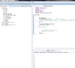
ut_read how i can set constant value '0' or '1' , and what i need to assign to FIFO wait_request.

Anyone please clarify me.
 

Attachments

  • Qsys_FIFO.JPG
    Qsys_FIFO.JPG
    165.3 KB · Views: 201
  • FIFO_Block.JPG
    FIFO_Block.JPG
    222.7 KB · Views: 207

Status
Not open for further replies.

Part and Inventory Search

Welcome to EDABoard.com

Sponsor

Back
Top