hari_preetha
Full Member level 2
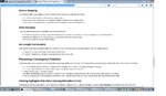
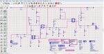
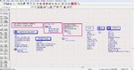
I am using Agilent Advanced Design System 2011.10 for my circuit design. I am getting the "no convergence error" for my designed circuit to obtain HB2 Two tone swept power. I have used "OPTIONS" setting also. Even though I used "OPTIONS" settings also, am getting the " no convergence error".
How to overcome this convergence problem for my designed circuit, latter I am able to obtain IIP3 measurement.
Herewith I attached the Schematic of my circuit, HB2 tone swept power simulation generated convergence error file, and solving convergence using "OPTIONS" setting file.
How to overcome this convergence problem for my designed circuit, latter I am able to obtain IIP3 measurement.
Herewith I attached the Schematic of my circuit, HB2 tone swept power simulation generated convergence error file, and solving convergence using "OPTIONS" setting file.