Continue to Site

Welcome to EDAboard.com

Welcome to our site! EDAboard.com is an international Electronics Discussion Forum focused on EDA software, circuits, schematics, books, theory, papers, asic, pld, 8051, DSP, Network, RF, Analog Design, PCB, Service Manuals... and a whole lot more! To participate you need to register. Registration is free. Click here to register now.

[ADS]method to establish correlation between LNA EM simulation and circuit simulation

Status
Not open for further replies.

pragash

Advanced Member level 2
Joined
Jul 4, 2005
Messages
512
Helped
64
Reputation
128
Reaction score
59
Trophy points
1,308
Location
Oakland
Activity points
4,940
it's often easy to design an LNA circuit by doing impedance matching using "Smith chart utility" tool in ADS. In the layout simulation, due to parasitic introduced by the layout, the layout simulation will not correlate to the circuit simulation. Is there any commonly used method of establishing a correlation between circuit and EM simulation for the LNA.

BR
pragash
 

The method is to optimize component values over layout that has already been simulated and characterized by s-parameters.
In order to do this, you should place optional ports ( for instance, a right place for a matching capacitor on a transmission line ) for components and creating parametric layout.
The second one is more difficult but efficient.The best method is to draw a "RF Good Layout".By doing this, your cut-n-try time decreases..
 
In order to do this, you should place optional ports ( for instance, a right place for a matching capacitor on a transmission line ) for components and creating parametric layout.

could you please explain this further? are you asking to measure parasitic inductance and capacitance of the each transmission line?
 

could you please explain this further? are you asking to measure parasitic inductance and capacitance of the each transmission line?
No, it's unrelated..
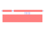
For instance, let's imagine a TL and L-C combined matching circuit.. And you're not sure the exact position of the Capacitor.So, you place optional ports for it then while doing circuit simulation you change the position of this capacitor and see the effect.
lay_test.png

I hope you understood what I meant..
 
I got what you mean now. actually, the layout follows good RF layout guidelines which avoid long interconnects and parallel ground plane underneath component pads and so on. However, parasitic inductor and capacitance are unavoidable at high frequency (2.5GHz) regardless of how good your layout is. my question is what can we do post layout to optimize the layout with parasitics. This is because component values given by "smith chart utility" is not giving good results. a method to optimize the layout to meet the performance.
 

I got what you mean now. actually, the layout follows good RF layout guidelines which avoid long interconnects and parallel ground plane underneath component pads and so on. However, parasitic inductor and capacitance are unavoidable at high frequency (2.5GHz) regardless of how good your layout is. my question is what can we do post layout to optimize the layout with parasitics. This is because component values given by "smith chart utility" is not giving good results. a method to optimize the layout to meet the performance.

You will solve these kind of problems by experimental methods.I cannot tell you now how a good RF layout is done here because learning layout tricks and hints takes so long time and you have to involve into many similar design to learn all.I'm RF Engineer with 30+ years experience and I do still not know all techniques and I'm still learning something everyday..
A hint : You may be inspired from well designed existing RF layouts from different App. Notes and Engineers..
 
I was looking for a methodology to optimize the circuit with parasitics. thanks for your input. I really appreciate it.
 

Status
Not open for further replies.

Part and Inventory Search

Welcome to EDABoard.com

Sponsor

Back
Top