Continue to Site

Welcome to EDAboard.com

Welcome to our site! EDAboard.com is an international Electronics Discussion Forum focused on EDA software, circuits, schematics, books, theory, papers, asic, pld, 8051, DSP, Network, RF, Analog Design, PCB, Service Manuals... and a whole lot more! To participate you need to register. Registration is free. Click here to register now.

Reference simulation problem

Status
Not open for further replies.

hktk

Junior Member level 3
Joined
Feb 2, 2005
Messages
27
Helped
2
Reputation
4
Reaction score
0
Trophy points
1,281
Activity points
263
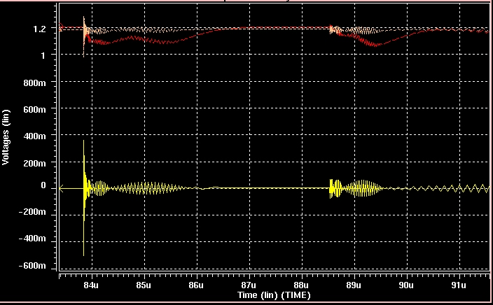
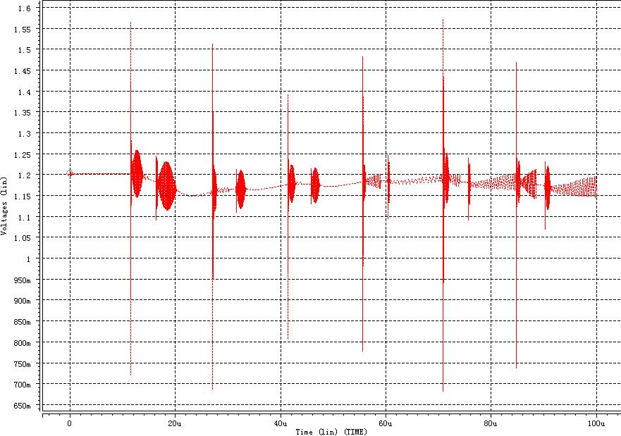
Hello, everyone. I meet a reference simulation problem and the following figure is the schematic and simulation results. When I put the reference circuit in the whole chip simulation with bonding model, the output of the reference has a large ripple with the switch frequency. When I just simulate the reference block, the loop characteristics are good enough. Can u guys give some advice about this? Hope for ur reply.

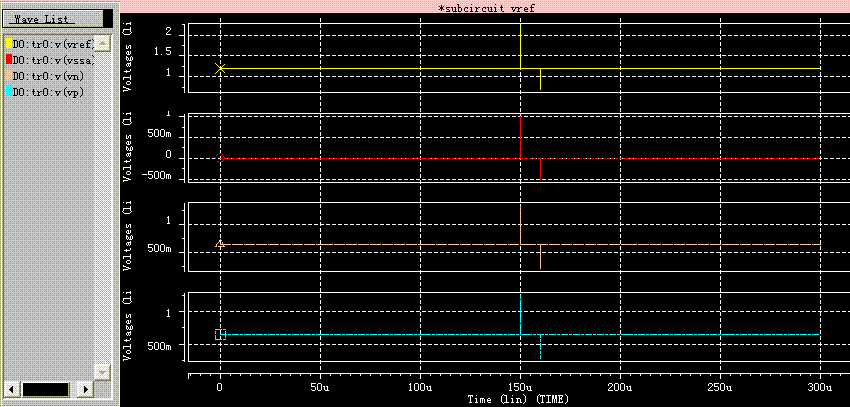
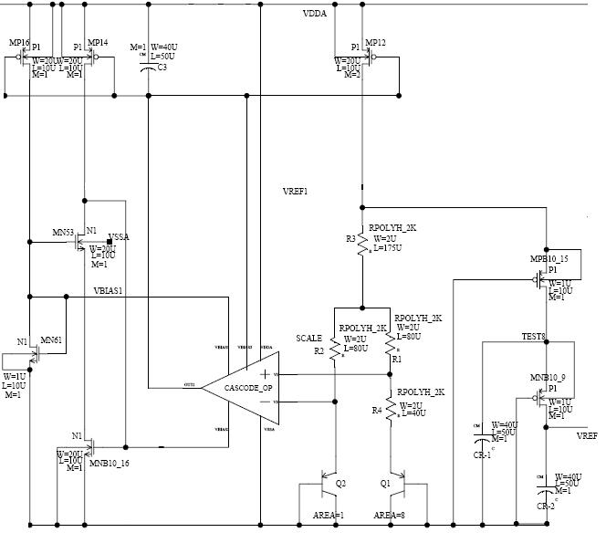
Schematic of Reference without start-up circuit
90_1168955798.JPG


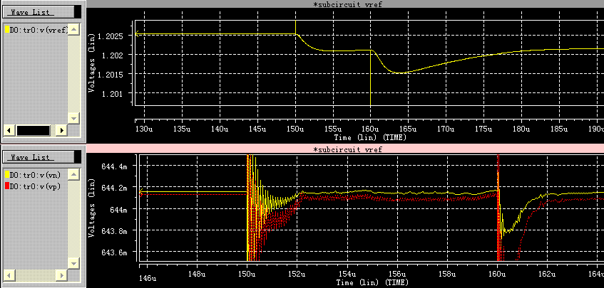
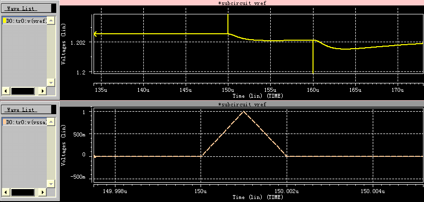
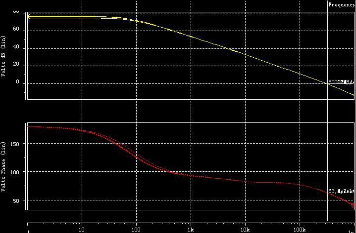
loop gain and phase simulation results
24_1168955841.JPG


Simulation Results in whole chip with bonding model
4_1168955909.JPG
 

There is 2 stage amplifier in closed loop of bgr. First one is cascode amplifier that output pole is dominant pole. Second one is MP12 with resistive and capacitive load.
Due to C3 u obtain stable loop for bgr only, when u connect addititional capacitance load at th ebgr output, u'll decrease second pole and have nonstable loop. Moreover C3 lead to poor psrr.

Possible solution:
1) Increase value of the C3 to obtain stable loop for maximum capacitive load. But this solution isn't good because u slow down transient response of ur circuit and obtain poor pssr.
2) Remove C3 and make miller frequency compencation from the drain of MP12. "Cascode miller compensation" is the best choice for u. Check stability at maximum capacitive load.
Regards
 

hi, DenisMark
I have tried the method you mentioned above, but the simulation result is the same as the figure posted. The load capacitor of the BGR output VREF is very small, so I think it can be neglected.
 

hktk said:
hi, DenisMark
I have tried the method you mentioned above, but the simulation result is the same as the figure posted. The load capacitor of the BGR output VREF is very small, so I think it can be neglected.
hi
plz remove the bonding pad ckt first, and then check the reference ckt only.
good luck
jeff
 

the reference is very good before adding bonding model. the chip is a boost converter. power ground and signal ground use the same pad VSSA. Bonding CKT connects VSSA and GND together.
 

Ok. Boost dc-dc :)
It looks like very big noise on power rails and poor psrr of bgr circuit.
My recomendation:
1) Use "cascode miller compensation", remove C3. C3 in ur schematic is a reason of poor psrr.
2) Check psrr of bgr.
3) Check stability of new bgr circuit. Also try transient analisys, to do this insert pulse voltage source in series with positive or negative pin of cascode amp.
4) Check noise value on the power rails (with bonding pad ckt). If it more than e.g. 200mV than the problem in ur design. Ur boost dcdc isn't good, because ur circuit makes a rapid current spikes though cupply rails. Thus u need find a source of that problem and resolve it (slow down some transients, make non-overlapping control, break-before-make technique,...). Or use addititional pins.
5) It's better to use NMOS isolated from substrate in analog blocks of ur dcdc. This decrease substrate coupling.
 

Split high power pad and analog block power pad.
 

here is our simulation result, the red line is the node VREF1 and the yellow one is the node VSSA with bonding. does the roll of the red line due to low loop gain or phase margin ?
56_1169113860.jpg
 

VSSA isn't as interesting as VDDA. What is VDDA?
What is the VDD value for ur design?
Do u try advices from my previous post?
Provide more information how u can?
 

C3 like a AC coupling cap, the ring transition of pwer by L is passed to the gate of M12, then the current of m12 is also ringing==> vref1 ring, too.
 

hi, DenisMark. the VDDA has a ripple of 30mv, and if without bonding, the noutput of BGR is OK.so i think the bad transient due to the VSSA with bonding. the most probable reason is the loop stability. where and how to break the loop? how to estimate the load effect?
 

I don't think that a propable reason is the loop stability. But I cann't indicate the reason bacause I haven't enough information from athor.
It looks like poor pssr capability of bgr ckt, or not proper biasing elements in bgr ckt, or some transients delive to bgr output (nonsituable load). In last case it's better to use buffer (amp with inity gain) between bgr ckt and a rest of dcdc.
It seems to me the last case is most propable.
wanily1983 if u are interested, u can break the loop at the positive input of cascode.
inp+----(~vac)---*---^^^1H---
.................................|
................................1F
.................................|
.................................VSSA
In such maner obtain dc solution and break circuit on ac (or insert verilog-a element in break point).
 

thank u, DenisMark,i will try the method u mentioned.

Added after 4 hours 47 minutes:

hi,DenisMark. i think the proper breaking point is the output node of OPAMP or the Positive input node of OPAMP, but the previous break method is hard to estimate the load effect. the dc gain of the two method should be the same. but when simulate, the previous method has a 60dB loop gain, but the last one only has 10dB.why do they have the different loop gain?
 

How to measure stability of OTA in BGR ckt is a vexed question.
Look for aryajur post on

I think that the method mentioned by me is correct because input capacitance of OTA is less than output. So we introduce minor mistake in closed loop gain estimation.
I'd lose a key moment in previous post. In addititional try to insert second break at negative input, but without ac voltage sourve.
I usually use verilog-a block for break loop during ac simulation. Previous solution more simple for realization.
 

hktk said:
here is our simulation result, the red line is the node VREF1 and the yellow one is the node VSSA with bonding. does the roll of the red line due to low loop gain or phase margin ?
56_1169113860.jpg


from ur graph, i think it is very important u have separate ground pad for ur reference circuit, i believe the noise is from ur swithing circuit. The best way is u have

example GNDA for reference circuit or other analog circuit.

GNDD for digital circuit ....


and be careful how place your layout in your chip.
 
Last edited by a moderator:

last night i checked the simulation results carefully and found it seemed the BGR oscilates at very high frequency about 500Mhz, as like the figure posted by hktk. it is almost the same if u remove the capacitor C3, i think it is because the C3 compensates the circuit at low frequency, the circuit is not stable at very high frequency due to the high frequency poles and zeros. how to solve this problem? any device is welcome.

Added after 39 minutes:

DenisMark, by the way, what is 'verilog-a block' you mentioned?
 

It seems to me u is mistaken. Ur bgr ckt very slow for 500MHz oscillation.
For help u I need more information about what u've done and what the results u've obtained.
Otherwise, it's useless to surmise.
I give u example of bgr ckt like yours with cascode miller compensation. It works ok.
('verilog-a block') See
I make test circuits in same maner.
 

Hi, DenisMark . we design this ref in a boost circuit. The output of the SMPS provide power supply to the control IC. now I post the simulation results of the ref which I add some pulse at vssa to replace the gnd with bonding. The simulation results are as following:

this is the ref output, the two inputs of OP,the vssa waves with constant vdda
29_1169636937.GIF


the detail waves of vref and the two inputs of OP
9_1169637102.GIF


the detail waves of vssa with a pulse disturbance
61_1169637197.GIF


why the vref roll down when the vssa has high frequency disturbance? when the vssa has many pulses like that(with bonding wire model), then the output of ref is as hktk posted.
 

Sorry, but I was very busy recently.
So, now we now that bgr ckt cann't oscillate at 500MHz. For dcdc ckt Vref from bgr ckt is used relatively to the VSSA potential. Due to ac coupled capacitor at bgr ckt output if VSSA changes relatively absolute ground than Vref must changes in same maner relatively absolute ground too. Relatively to VSSA Vref must keeps close to constant.
I'm in doubt with some moments:
1) I see that u have large transients on VSSA rail (~1V). it's not accaptable for clear reference. u should to maximum separate VSSA from power VSS and digital VSS.
2) I see that transient on Vref don't copy transient on VSSA. It looks like some load applied to bgr ckt output. Yours bgr ckt don't assume some resistive load and switched capacitance load (e.g. comparator, another input of which changes rapidly). Check this issue.
3) It seems to me that transitors MPB10_15 & MNB10_9 isn't usefull because thier make worse load regulation of bgr ckt.
 

Status
Not open for further replies.

Part and Inventory Search

Welcome to EDABoard.com

Sponsor

Back
Top