Continue to Site

Welcome to EDAboard.com

Welcome to our site! EDAboard.com is an international Electronics Discussion Forum focused on EDA software, circuits, schematics, books, theory, papers, asic, pld, 8051, DSP, Network, RF, Analog Design, PCB, Service Manuals... and a whole lot more! To participate you need to register. Registration is free. Click here to register now.

Advice sought for Post place and route glitches!!

Status
Not open for further replies.

sixdegrees

Junior Member level 2
Joined
Jul 21, 2006
Messages
20
Helped
0
Reputation
0
Reaction score
0
Trophy points
1,281
Activity points
1,501
error posedge , 800ps

Hello,
I am using a Spartan 3 FPGA board and am having problems in the Post Place n Route simulation using Xilinx ISE 7.1i and ModelSim XE 6.0a.I have unnecessary glitches which causes garbage outputs before the output finally settles. Not only in large designs(I am designing IP core for a DSP proc.) if i instantiate a simple register,the post PnR simulation results shows glitches.

Below is the code and testbench for a simple 8bit register.

`timescale 1ns / 1ps

module top(in, clk, reset, enb, out);

input [7:0] in;
input clk;
input reset, enb;

output [7:0] out;

reg [7:0] out;

always @(posedge clk)
begin
if(reset)
out <= 8'b0;
else if(enb)
out <= in;
else
out <= out;
end


endmodule

module test_top_v;

// Inputs
reg [7:0] in;
reg clk;
reg reset, enb;

// Outputs
wire [7:0] out;

// Instantiate the Unit Under Test (UUT)
top uut (
.in(in),
.clk(clk),
.reset(reset),
.enb(enb),
.out(out)
);
always #25 clk = ~clk;
initial begin
// Initialize Inputs
in = 0;
clk = 0;
enb = 0;
reset = 1;

// Wait 100 ns for global reset to finish
#100;
#50 reset=0;

// Add stimulus here

#50 enb = 1;
in = 8'b00000001;
#50 enb = 0;

#180 enb = 1;
in = 8'b11111111;
#50 enb = 0;
#100 $stop;
end


endmodule

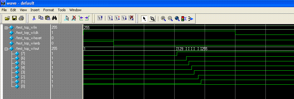
I get output glitches when the 'in' values changes from 8'h1 to 8'hFF.

Can someone plz give me some advice on how to get around all these problems and any links/pointers to get a robust and perfect design. I seem to get the idea that FPGA coding for implementation is quite a different ballgame as regards to functional simulation

Kool
 

I routed your design with ISE 8.1.03i and did a post-route simulation in ModelSim 6.2a. I don't see any problem.

Be careful not to cause a hold-time violation. Your 'in' changes to 255 only a few nanoseconds after the clock. That's usually fine, but depending on your IOB configuration, flop location, and clock/signal routing, it could be a problem.

Be sure to install the latest service pack for 7.1i. Version 7 started out very buggy.
 

Hi!
Thanks for taking the trouble.
I am attaching the simulation waveform which I got.Please see the attached jpg file.
I am using ISE 7.1i Service Pack 4 and dont knw whether I should use 8.1i or not.

Please clarify
 

No problem! You are simply seeing the different propagation delays from your 8-bit 'out' register to the output pads. Your router probably placed the register into the input IOBs (thereby providing predictable input setup/hold timing), so the routes to the output pads have different lengths. Use FPGA Editor to see the physical layout.

To see the delays more clearly in ModelSim, expand the individual bits and zoom in horizontally. Below is my display with 1ns grid.

Maybe you could add an output register to your design. Then all your input and output signals will have sharp timing and immunity to routing delays. Also, see the IOB constraint in your Constraints Guide.

By the way, if you trim your JPEG or GIF to 800 pixels wide, it will display automatically.
 

Hi @echo47

I have used a custom UCF file and I don't think there is any probability of router placing the OUT with IN values. Also I assume you have seen my attached waveform because I can definitely see a glitch there.

The ucf for Spartan 3 XC3s5000 based board is :

#PACE: Start of PACE I/O Pin Assignments
NET "clk" LOC = "AH15" ;
NET "reset" LOC = "AG26" ;
NET "in<0>" LOC = "AH29" ;
NET "in<1>" LOC = "AJ27" ;
NET "in<2>" LOC = "AJ26" ;
NET "in<3>" LOC = "AJ25" ;
NET "in<4>" LOC = "AK24" ;
NET "in<5>" LOC = "AK23" ;
NET "in<6>" LOC = "AK22" ;
NET "in<7>" LOC = "AJ20" ;
NET "out<0>" LOC = "E8" ;
NET "out<1>" LOC = "E9" ;
NET "out<2>" LOC = "F11" ;
NET "out<3>" LOC = "F12" ;
NET "out<4>" LOC = "F13" ;
NET "out<5>" LOC = "F14" ;
NET "out<6>" LOC = "E15" ;
NET "out<7>" LOC = "F16" ;

30_1166414372.GIF
 

(I added a few more words to my previous message.)

Your new expanded waveform clearly shows the different propagation delays. The register is definitely not in the output IOBs. It's either in the input IOBs or in the logic fabric. Try FPGA Editor - I find it extremely valuable for understanding the place-and-route behavior. Also see your "IOB Properties" in your "Mapping Report File" - it shows which IOBs have assigned registers.

Your "LOC" constraints specify only the pin numbers. They don't control where the router puts the register.

I see you found another way to insert an image into your message!
 

So please tell me how do I know whether my design is proper or not, whether I am having a glitch or not and how to make this register values go to output instead or in the IOB's or logic fabric as you mention. Also I can see the value of 87 in your 'out' signal which definitely shouldnt be there I think. Please clarify if that is supposed to be there.

Also I am quite confused about how to get around the setup and hold violations which I am getting. Is there any way to understand the exact registers which are having those violations. My ModelSim seems to give only messages like:

Error: C:/Xilinx/verilog/src/simprims/X_FF.v(52): $hold( posedge CLK:492572 ps, posedge I &&& (in_clk_enable == 1):492807 ps, 381 ps );
# Time: 492807 ps Iteration: 2 Instance: /tb_reg_file_v/uut/Ram_2_38_3110

But I cannot understand what does that 52 in the Error means and what is this X_FF.v file,and how can I get around this problem.

And everyone seems to start somewhere, I have been here for a couple of days so will gradually catch up.

Added after 23 minutes:

And also the IOB properties are attached herewith:

Section 6 - IOB Properties
--------------------------

+------------------------------------------------------------------------------------------------------------------------+
| IOB Name | Type | Direction | IO Standard | Drive | Slew | Reg (s) | Resistor | IOB |
| | | | | Strength | Rate | | | Delay |
+------------------------------------------------------------------------------------------------------------------------+
| clk | IOB | INPUT | LVCMOS25 | | | | | |
| enb | IOB | INPUT | LVCMOS25 | | | | | |
| in<0> | IOB | INPUT | LVCMOS25 | | | INFF1 | | IFD |
| in<1> | IOB | INPUT | LVCMOS25 | | | INFF1 | | IFD |
| in<2> | IOB | INPUT | LVCMOS25 | | | INFF1 | | IFD |
| in<3> | IOB | INPUT | LVCMOS25 | | | INFF1 | | IFD |
| in<4> | IOB | INPUT | LVCMOS25 | | | INFF1 | | IFD |
| in<5> | IOB | INPUT | LVCMOS25 | | | INFF1 | | IFD |
| in<6> | IOB | INPUT | LVCMOS25 | | | INFF1 | | IFD |
| in<7> | IOB | INPUT | LVCMOS25 | | | INFF1 | | IFD |
| out<0> | IOB | OUTPUT | LVCMOS25 | 12 | SLOW | | | |
| out<1> | IOB | OUTPUT | LVCMOS25 | 12 | SLOW | | | |
| out<2> | IOB | OUTPUT | LVCMOS25 | 12 | SLOW | | | |
| out<3> | IOB | OUTPUT | LVCMOS25 | 12 | SLOW | | | |
| out<4> | IOB | OUTPUT | LVCMOS25 | 12 | SLOW | | | |
| out<5> | IOB | OUTPUT | LVCMOS25 | 12 | SLOW | | | |
| out<6> | IOB | OUTPUT | LVCMOS25 | 12 | SLOW | | | |
| out<7> | IOB | OUTPUT | LVCMOS25 | 12 | SLOW | | | |
| reset | IOB | INPUT | LVCMOS25 | | | | | |
+------------------------------------------------------------------------------------------------------------------------+


It clearly shows that out are output IOBs and neither input IOB or logic fabric as you mention, in fact I am quite surprised at the fact that a clearly specified output will be remapped as input after Mapping, I am not aware of any router that does that, I may be wrong so please elaborate your justification a little with any examples.
 

These unequal propagation delays are called "skew". (A "glitch" is a somewhat different phenomenon.) Skew occurs everywhere in the real world to some degree, so it's very common to see weird bus values for a few hundred picoseconds. That actually happens inside the FPGA, and it's perfectly normal. We engineers avoid skew-related headaches by using synchronous design.

Your design seems proper, unless your destination device requires tighter skew control. If it does, then you can add a register to the output IOBs.

When you run a post-route simulation. Your netlist gets expanded into a large extremely detailed HDL file full of low-level Xilinx primitives. Look for this file in your project folder. It can be very difficult to recognize your original design in this file, but that's what ModelSim is simulating. Your error message is referring to a timing problem with an X_FF flip-flop primitive named /tb_reg_file_v/uut/Ram_2_38_3110. The "52" refers to a line number in Xilinx's Verilog model describing that flip-flop's behavior.

Your mapping report shows *input* registers. That's what "INFF1" means in the Reg(s) column. The mapper can put registers in places that may seem surprising but are functionally correct. These place may be unrelated to your signal names (such as "in" and "out") or your Verilog port directions (such as "input" and "output"). If you want to nail down the register location, you must use constraints.

By the way, I very rarely run post-route simulations. I normally create a fully synchronous design, and run behavioral simulations. Then I specify a clock constraint, run place-and-route, and if it meets timing I'm done.
 

Hi echo47!

I am really grateful to you for this wonderful interaction,I really appreciate your help

Since you mentioned that the only way to get tight skew control is to use a fully synchronous design, and I cant allow skew to be there in my design, can u plz give me the code as you would have done it so that I can understand where am I going wrong with my stuff. I know its very basic but I think basics are all that matters in a big design. And also what do u mean by specifying constraints on registers,can u please tell me how to to do that and the complete design flow as you might pursue so that I can get a feel of the things.

Thanks for your help!!
 

Synchronous design tolerates the skew on data signals, it does not necessarily control the skew. It clocks all your flops simultaneously, so your design works reliably despite many different propagation delays. (The clock net must have low skew.)

Your second simulation display doesn't show the time scale. My simulation shows about 800ps of skew. That's not very much. Is it really causing you a problem?

You can minimize the output skew by using the output IOB registers. This eliminates routing delays from the output timing. You probably want to maintain the input IOB registers because they provide nice predictable input setup/hold timing. So we need two 8-bit registers in the HDL. Your Xilinx mapper should be smart enough to automatically place one of them into the input IOBs, and the other one into the output IOBs. (Beware, that default mapper behavior is configurable.) Of course, the new register will delay the data by one clock cycle.
Code:
module top (in, clk, reset, enb, out);
  input       [7:0] in;
  input             clk;
  input             reset, enb;
  reg         [7:0] a;    // the mapper should place this into the input IOBs
  output reg  [7:0] out;  // the mapper should place this into the output IOBs

  always @ (posedge clk)
  begin
    if (reset)
      a <= 8'b0;
    else if (enb)
      a <= in;
    else
      a <= a;
    out <= a;
  end
endmodule
The mapping report now shows input and output registers INFF1 and OFF1:
Code:
Section 6 - IOB Properties
--------------------------

+-------------------------------------------------------------------------------------------+
| IOB Name | Type | Direction | IO Standard | Drive    | Slew | Reg (s)  | Resistor | IOB   |
|          |      |           |             | Strength | Rate |          |          | Delay |
+-------------------------------------------------------------------------------------------+
| clk      | IOB  | INPUT     | LVCMOS25    |          |      |          |          |       |
| enb      | IOB  | INPUT     | LVCMOS25    |          |      |          |          |       |
| in<0>    | IOB  | INPUT     | LVCMOS25    |          |      | INFF1    |          | IFD   |
| in<1>    | IOB  | INPUT     | LVCMOS25    |          |      | INFF1    |          | IFD   |
| in<2>    | IOB  | INPUT     | LVCMOS25    |          |      | INFF1    |          | IFD   |
| in<3>    | IOB  | INPUT     | LVCMOS25    |          |      | INFF1    |          | IFD   |
| in<4>    | IOB  | INPUT     | LVCMOS25    |          |      | INFF1    |          | IFD   |
| in<5>    | IOB  | INPUT     | LVCMOS25    |          |      | INFF1    |          | IFD   |
| in<6>    | IOB  | INPUT     | LVCMOS25    |          |      | INFF1    |          | IFD   |
| in<7>    | IOB  | INPUT     | LVCMOS25    |          |      | INFF1    |          | IFD   |
| out<0>   | IOB  | OUTPUT    | LVCMOS25    | 12       | SLOW | OFF1     |          |       |
| out<1>   | IOB  | OUTPUT    | LVCMOS25    | 12       | SLOW | OFF1     |          |       |
| out<2>   | IOB  | OUTPUT    | LVCMOS25    | 12       | SLOW | OFF1     |          |       |
| out<3>   | IOB  | OUTPUT    | LVCMOS25    | 12       | SLOW | OFF1     |          |       |
| out<4>   | IOB  | OUTPUT    | LVCMOS25    | 12       | SLOW | OFF1     |          |       |
| out<5>   | IOB  | OUTPUT    | LVCMOS25    | 12       | SLOW | OFF1     |          |       |
| out<6>   | IOB  | OUTPUT    | LVCMOS25    | 12       | SLOW | OFF1     |          |       |
| out<7>   | IOB  | OUTPUT    | LVCMOS25    | 12       | SLOW | OFF1     |          |       |
| reset    | IOB  | INPUT     | LVCMOS25    |          |      |          |          |       |
+-------------------------------------------------------------------------------------------+
The post-route simulation will now show probably zero output skew. The actual FPGA device will have a small output skew, usually a small fraction of a nanosecond, due to manufacturing variations and other small effects that the simulation models don't include.

To learn more about constraints, please refer to the ISE Constraints Guide. I won't try to summarize that enormous complex book! A good starting point may be the IOB constraint, since it is related to our discussion.
 

    sixdegrees

    Points: 2
    Helpful Answer Positive Rating

Attachments

  • output.jpg
    output.jpg
    48.8 KB · Views: 98
  • schematic.jpg
    schematic.jpg
    48 KB · Views: 101

so is the result normal?
 

Looks pretty normal to me. This is post place & route, right? Then the simulator will take into account all the routing & logic delays. Which is why you see the transitions. Some bits of the sum output transition faster than others, due to how everything is physically placed.

PS: could you use .png instead of .jpg for screenshots? That makes it a bit easier to read. :)
 
  • Like
Reactions: krys

    krys

    Points: 2
    Helpful Answer Positive Rating
Status
Not open for further replies.

Part and Inventory Search

Welcome to EDABoard.com

Sponsor

Back
Top