suhas_shiv
Full Member level 2
Hi all,
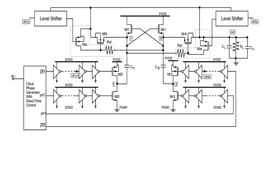
I am designing a switched capacitor Voltage Doubler as shown in the attached figure. Its based on the cross-coupled configuration. The problem i am facing is that the 2 nmos transistors (cross coupled) are always off because the Vgs=0. How do I bias them so that they are on? If possible can someone explain how I go about designing the circuit? Thanks.
Also I am using non-overlapping clocks ( from 0 to Vdd=5V). Is that enough to turn on the transistors or do I need to specify any DC voltage(like an offset) to bias them?
I am using 0.25um TSMC technology.
Thanks