Continue to Site

Welcome to EDAboard.com

Welcome to our site! EDAboard.com is an international Electronics Discussion Forum focused on EDA software, circuits, schematics, books, theory, papers, asic, pld, 8051, DSP, Network, RF, Analog Design, PCB, Service Manuals... and a whole lot more! To participate you need to register. Registration is free. Click here to register now.

sizing of floating current sources in folded cascode amplifier ?

Status
Not open for further replies.

cmos_ajay

Full Member level 2
Joined
Jan 30, 2007
Messages
126
Helped
0
Reputation
0
Reaction score
0
Trophy points
1,296
Activity points
2,247
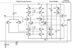
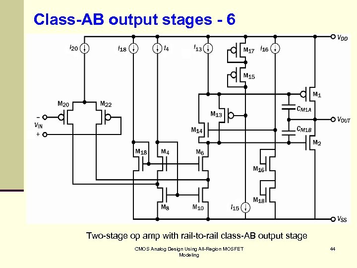
The attached picture shows a folded cascode amplifier with class AB o/p stage.
* How should I select the W/L of the mosfets MP7, MN5, MP8 and MN6 ?

* Suppose this amplifier architecture has a fully differential o/p.
Assume that only the tail current PMOS source Ib1 , input diff pair devices MP1, MP2 are 5 volt.
The remaining transistors are of 1.8V devices.

Can someone suggest a common mode feedback circuit for such a circuit with 5V and 1.8V devices ? A schematic diagram will be helpful .
 

Attachments

  • foldcas - Copy.PNG
    foldcas - Copy.PNG
    72.3 KB · Views: 552

* How should I select the W/L of the mosfets MP7, MN5, MP8 and MN6 ?

You would rather want to size them in a following manner:
P7 = P8
N5 = N6

By selecting W/L of N6 and P8, you set the gate voltages of output transistors N9 and P11. Hence you are rather looking for such situation, where:
- ID_N6 = ID_P8 = 1/2 ID_P6
- output quiescence currents ID_N9 = ID_P11 have the desired values


Can someone suggest a common mode feedback circuit for such a circuit with 5V and 1.8V devices ?
What exactly do you need CMFB circuit for?
 

I agree with your suggestions.
If I am using a 0.18um process, what should be the typical length of mosfets MP8 and MN6 ??
Can they be replaced by a resistor ??
 

If I am using a 0.18um process, what should be the typical length of mosfets MP8 and MN6 ??

It is a hard question due to the complexity of your architecture. Start with L = Lmin or L = 2 x Lmin so for high voltage domain 3.3V that would be 0.35 um or 0.7 um, respectively.
Why you are using such architecture? Cannot you start with the simpler variation of your architecture and then successively modify it to obtain your final architecture? If you can, try to start with a simpler variation of your architecture for example:

opamp.png

Source: https://payhip.com/b/5Srt (paid version)


US07414473-20080819-D00000.png


Source: https://patentimages.storage.googleapis.com/US7414473B1/US07414473-20080819-D00000.png


image-44.jpg


Source: https://present5.com/presentation/d2e3428f7a24e8334a0fbccc40bf1e0c/image-44.jpg

For example: try to use one AB control stage and one current mirror. Then add another current mirror and AB control stage.


Can they be replaced by a resistor ??
Generally speaking, yes you can. However, the behaviour of your opamp may not be as expected. That is, the class AB behavior may not be sufficient. Try to simulate AB control stage, that is, your P8 and N6 with two current mirrors. You will see how nicely this stage operates, that is, for differences between current sources, sources of P8 and N6 are close to each other what enables your output transistors P11 and N9 to be fully opened when another one is closed (e.g. P11 opened and N9 closed or P11 closed while N9 opened).
 

Status
Not open for further replies.

Part and Inventory Search

Welcome to EDABoard.com

Sponsor

Back
Top