Continue to Site

Welcome to EDAboard.com

Welcome to our site! EDAboard.com is an international Electronics Discussion Forum focused on EDA software, circuits, schematics, books, theory, papers, asic, pld, 8051, DSP, Network, RF, Analog Design, PCB, Service Manuals... and a whole lot more! To participate you need to register. Registration is free. Click here to register now.

Frequency characteristics of op amp

Status
Not open for further replies.

DavidYebadlo

Junior Member level 1
Joined
Apr 6, 2020
Messages
17
Helped
0
Reputation
0
Reaction score
0
Trophy points
1
Activity points
177
Hi.
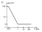
I designed a system with an operational amplifier that must meet the following frequency characteristics:
charakterystyka.png
My layout diagram in LTspice
schematltspice.png
and it's the characteristic:
charltspice.png
Should I change the voltage source in the schematic? And what type should I change to? Electronic components and their parameters in this system are selected correctly, so it is not their fault.
Thank you in advance for your help!
 

Why would you think that changing external stimulus would change the response of your circuit? It’s a sine wave, right? How do you know the components are selected correctly? First of all, it looks like a completely impractical circuit. A 10H inductor?? Where did you get this circuit from?
 

It's my homework and i know it's (maybe) good because my lecturer said the project is ok but now i have to make a simple simulation and i don't know if the voltage source parameters is good or not.
 

It is OK but as stated, completely impractical. If you built it, expect it to be the size of a house brick and weigh several Kg because of the amount of iron in the inductor cores.

Instead of using series inductors experiment with parallel capacitors to get the same effect. The values would then make it practical as a real circuit. I'm worried your tutor asks you to build it to verify the simulation!

Brian.
 

The graph shows numbers for its vertical. Are they the amount of gain? Then -1 is an inverting gain of 1 and -100 is an inverting gain of 100 times? Usually a graph like this is measured in decibels.
The horizontal has kHz. Why doesn't it begin with 20Hz (instead of 0.02kHz)?

It looks like the level reduces 34dB for 6 octaves which is 5.67db per octave which is about the same as a simple RC lowpass filter. It is made with an inverting opamp using 2 resistors producing an inverting very low frequency gain of 50 (34dB) plus an RC (a capacitor in series with a resistor) parallel with the negative feedback resistor.
 

Your plot doesn't look right. What point are you plotting? You should be plotting the output. It should look like this:
worlds heaviest circuit.png
 

Almost. 1kHz and higher should have a gain of +6dB (2 times), not 0dB.

The plot came from the simulation. I'm too lazy to actually do the analysis by hand. How do you know it should be gain of 2, other than from the initial (suspcicious) plot?
 

Post #6 plot shows Vout, not gain. Specified gain and actual gain of post #1 schematic are however different. I presume, the circuit should be corrected to follow the spec.

Finally implementing the schematic with large inductors is very impractical. Why not use an RC circuit?
 

Ok, I plotted gain. It STILL doesn't look like the OP's plot. Or the "ideal" plot. But, here's the problem: OP has defined the sine source with a 2 Volt offset, it should be zero. This seems like a bug in LTSpice to me. When you define a sine voltage source, the left side of the window is where you enter frequency, offset, amplitude, start time, etc., etc. On the right side of the window you define the "small signal AC analysis parameters": Amplitude and phase. One would think that those are the only two parameters that matter for AC analysis, but apparently not.

worlds heaviest circuit2.png
 

If I understand right, the post #1 circuit doesn't work due to the 2V DC offset defined in the SIN source. It drives the OP output to the rails.

The general point to observe, you need to check DC operation point in AC analysis with active components.
 

EDIT:
How can the simulation have a 20Hz sinewave (its peak is 20V!) AND a frequency sweep at the same time?
 

It can't. The 20 Hz SIN voltage is used in .TRAN and the sweep in .AC analysis.

- - - Updated - - -

For the record, the specified gain is achieved with the given resistor values and L1=0.8, L2=1.6. As previously stated, SIN offset must be removed.
 

Solving the circuit by hand is very simple (considering all components as ideal), since the gain of the proposed configuration is G=-Zfeedback/Zseries then:

|G| = -abs[ (R2 + jwL2)/(R1 + jwL1) ]

From this we can see that G(0) = -R2/R1 and G(infinite) tend to -L2/L1. Using the values of the assignement R2/R1 = 100 and L2/L1 =2
L2/L1 = 2 is not met in the proposed schematic that shows instead 0.5 (could by a typo).

In order to calculate all the value we can use the -3dB frequency f = 1/(2*pi*L/R) so that if we set arbitrary R1 to 100 ohm then:

R2 = 10k
L1 = 100/(2*pi*20) = 0.796 H
L2 = 1.59 H

That are the same values found by FvM. At these two frequencies (20Hz and 1k) we will not have the required values but at 20 Hz we will have -100/sqrt(2) = -70.7, while at 10k we will have -2*sqrt(2) = -2.8. Furthermore we have not enough degrees of freedom to fix both lower and higher frequency amplitudes. I've checked before the pairs (20Hz,-100) and (1k, -2) are consistent.
 

Status
Not open for further replies.

Similar threads

Part and Inventory Search

Welcome to EDABoard.com

Sponsor

Back
Top