Continue to Site

Welcome to EDAboard.com

Welcome to our site! EDAboard.com is an international Electronics Discussion Forum focused on EDA software, circuits, schematics, books, theory, papers, asic, pld, 8051, DSP, Network, RF, Analog Design, PCB, Service Manuals... and a whole lot more! To participate you need to register. Registration is free. Click here to register now.

best location to place an analogue multipleoxor

Status
Not open for further replies.

flote21

Advanced Member level 1
Joined
Jan 22, 2014
Messages
411
Helped
1
Reputation
2
Reaction score
3
Trophy points
1,298
Activity points
5,595
Hi guys!

I am designign an analogue stage with some opamp to adapt voltage levels and i need to use a multiplexor. My question is where is the best location for this component:

Option 1: Input Voltage => OpAmps voltage adaptation => Mux => ADC
Option 2: Input Voltage => Mux => OpAmps voltage adaptation => ADC

Thanks in advance!
 

Hi,

another question for "best"....

Maybe you should tell us what you mean with "best".

It could be: cost, board space, sampling speed, offset, cross talk, precision....and many other ...


Klaus
 

Hi!
I need high percision and low cost mostly ..

Greetings
 

Hi,

Precision: depends ( expected precision, timing, supply, signal, impedances .... the usual precision determing parameters)
Cost: 2

Klaus
 

Hi,

how does your input signal looks like? Single continuous wave (CW) frequency? Amplitude?
Which kind of mixer do you want to use? Active or passive? What's the mixer's conversion loss or gain? Mixer application, IF or direct-down conversion?

According to Friis formula of noise, you should place the amplifier/opamp before your mixer. Other way arround your mixer noise is also amplified.
Further, if you are realizing a direct-down conversion (zero-IF) also a possible DC offset caused by a local oscillator leakage will be amplified by an amplification after your mixing stage.

As KlausST already stated, option 2 is cheaper as you have lower requirements for your opamp ciruitry e.g. bandwidth and slew rate.

greets
 

if all of your inputs are always in the same range and always get processes the same way, then mux first, and one op amp circuit

if your inputs are not always in the same range and always must get processed differently, then op amps first, them mux.
i did this for built in condition reporting - voltages and currents for the device in several different ranges.
 

Hello guys.

Thanks for your replies. The application is about monitoring DC currents sensors using HALL effect curret sensors (LEM manufacturer) which gives you an output voltage in the range of +-4V

Then I need to adapt the output voltage of the current sensor to the ADC input range (0-2v5) of the microcontroller. But I don't have enough ADC inputs in the uC to monitor all the currents and I need several multiplexors.

Therefore, I would like to know if placing the muxes between the sensor output and the ADC inputs is a good practice or it is not recommended. This question is because I had a look to other designs and those designs adapt firstly the sensor output voltage and they use the mux later just before the ADC. Is there any Gode reason of doing that?

Finally I don't have hard timing requirements to monitor these signals (500 ms is the mux speed). As I commented previously, it is most important to have an accurate and clean measurement over other requirements.

Thanks everyone
 

what is the supply range of your mux? your op amp?

if the mux supply range and the op amp supply rnage is greater than +/- 4V, then mux than opamp then uP.
since all of your samples are in the same range, mux first, then scaling op amp, then uP.

If the mux supply is not greater than +/- 4V or if the opamap supply range is not greater than +/- 4V,
youll have to do the scaling in each channel first.

Basically, configuration will depend more of properties of the Hall Effect devices, the op amps, the mux, and the uP
 

If source impedance is high then mux leakage
and capacitance can bother the signal.

If destination impedance is low then some muxes
are not good (on resistance tends to be high,
compared to analog switches).

If signals come via a harness which can see
electrical faults, overvoltage-protecting muxes
can save having to add protection components.

If it's possible to use cheap ADCs one per
sensor and multiplex (or simply poll) on the
digital side, that might be cleanest. Maybe a
SPI or I2C ADC exists that suits your needs?
Consider the "sensor" as the Hall, ADC and
bus interface if any?
 

Hi,

Post#1: no specification
Post#3: no specification
Post#7: +/-4 V --> 0...2.5V, 500ms
No circuit, no part values, no other specifications...

--> use some Rs to adjust voltage range and use a single MUX, nothing else, no Opamp.
Simple, low cost, high precision.

If you want more detailed answers you need to provide complete infornations first.

Klaus

PS:
look through the previous posts:
Every "If" tell that we are guessing.
Every question mark tells you we need more informations
Both tells you that the answer may or may not fit to your problem.
 

Hi,

how does your input signal looks like? Single continuous wave (CW) frequency? Amplitude?
Which kind of mixer do you want to use? Active or passive? What's the mixer's conversion loss or gain? Mixer application, IF or direct-down conversion?

According to Friis formula of noise, you should place the amplifier/opamp before your mixer. Other way arround your mixer noise is also amplified.
Further, if you are realizing a direct-down conversion (zero-IF) also a possible DC offset caused by a local oscillator leakage will be amplified by an amplification after your mixing stage.

As KlausST already stated, option 2 is cheaper as you have lower requirements for your opamp ciruitry e.g. bandwidth and slew rate.

greets

Ok that reply was totally useless. It was defenetifely too late and I mixed it up with an analog mixer :-?. Sorry for that.

If your LEM output voltage is in the range of ±4 V, there is no need for an opamp if your are only interested in amplification. If you are implementing some kind of substraction or addition in the analog domain, due to the lack of simultenous access to your ADC inputs it makes sense to me. Maybe you are using an instrumentation amplifier to supress common mode noise and not burdn your sensors (I do not know if that is a topic for Hall effect sensors)?! Please tell us what are you planing to do with your opamps.

Further, keep the supply voltage of your switches in mind. As you are observing a signal with negative and positive voltage "swing", a DC bias is required (here your opamp may be used). There are also switches which are capeable to be operated with a single supply, while handling positive and negative voltages which are larger than the applied supply voltage. Those so-called Beyond-the-Rails switches are manufactured by MAXIM [1].


[1] https://www.maximintegrated.com/en/...g-switches-multiplexers/beyond-the-rails.html

greets
 

Hi everybody!

I will try to give a deteail explanation about the design I want to do.

The requirements are:

1) Use 38 hall effect current sensors to monitor the DC currents of photovoltaic strings. The model of the current sensor used is: LEM HTA 300-S
2) Use the uC ATSAME54P20A to capture and process the data.

According to the previous requiremnts there are two issues:

1) The uC ATSAME54P20A provides 32 ADC inputs. And I need to sample 38 currents. Therefore the uC has not enough ADC inputs to cover the first requirement.
2) The output HTA 300-S current sensor is +-4V (denpens of the direction of the current) and the range if uC ADC inputs goes from 0V to 2.5V. So I need to scale the output sensor voltage to fits with the ADC input range because when I process the data in the uC, I need to detect direction and value of the current through RS.

In order to solve the second issue, my plan to scale the output sensor voltage is implementing a signal conditioning circuit like this:

OpAmpScheme.png

(I am open to other possibilites to scale the signal. So any other proposal will be very welcome)

However, in order to solve the first issue, I have in my head three different solutions and I don't know which is better to get a good compromise between accuracy and cost effciency:

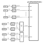
1) Solution 1: Drive 30 currents measurents directly to the uC through the OpAmp stage. And drive 8 current measurements through the opamp stage firstly and place two 4:1 Mux in a second stage before driving the measurement to the ADC inputs:

Solucion1.png

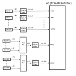
2) Solution 2: Drive 30 currents measurents directly to the uC through the OpAmp stage. And drive 8 current measurements through 4:1 Mux stage firstly and place the opamps in a second stage before driving the measurement to the ADC inputs (Notice the are bipolar Mux available in the market):

Solucion2.png

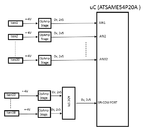
3) Solution 3: Solution 1: Drive 32 currents measurents directly to the uC through the OpAmp stage. And drive 6 current measurements through the opamp stage firstly and place a I2c or SPI external ADC connected to a digital communication port of the uC:

Solucion3.png

(I also open to other solutions)

I hope now you can undersand it better.

Thanks
 

Hi,

Some good informations ... that enables us to give you more detailed assistance.

***
38 sensors. Good to know. Because it´s a big difference whether you need 1 OPAMP or 38 OPAMPs. (it´s not that big difference if we talk about two channels)
So every tiny reduce in complexity will have big impact on overall complexity.

Use the uC ATSAME54P20A to capture and process the data.
What´s your sampling rate per channel
and what´s the sampling scheme:
like
Ch1 - Ch2 - Ch3 - Ch1 - Ch2 - Ch3 - Ch1 - Ch2 - Ch3 -(channels interleaved)
or:
Ch1 - Ch1 - Ch1 - Ch2 - Ch2 - Ch2 - Ch3 - Ch3 - Ch3 - one channel after the other. How many samples per channel
or any other

Also: What´s the ADC reolution? and what accuracy and what precision of your calculated values do you expect?

1) The uC ATSAME54P20A provides 32 ADC inputs. And I need to sample 38 currents. Therefore the uC has not enough ADC inputs to cover the first requirement.
My style is to treat all inputs most equally, thus I´d rather use just 5 ADC channels and 5 pieces of 8-to1-Demux. But that´s a personal taste.

The output HTA 300-S current sensor is +-4V (denpens of the direction of the current) and the range if uC ADC inputs goes from 0V to 2.5V. So I need to scale the output sensor voltage to fits with the ADC input range because when I process the data in the uC, I need to detect direction and value of the current through RS.
(I have quite a lot of experience with the HTAxxx Current transducers. Regulation loops down to some 10s of mA AC with a HTA1000. DC stability is worse, especially when you expect some overcurrent peaks --> remanence effects)
There are several solutions to this.
For 38 channels... I´d go this approach:
Generate one common and stable ADC_VRef/2 reference ( = 1.25V. And yes, directly derived from the ADC_reference) and use this signal as "GND" for all the HTA300. Then all your DC_level_shift is done. No OPAMP needed at all, just a couple of Rs and Cs.
While the HTA300 will be happy with the 1.25V (2.5V) unsymmetry in supply voltage you may go the clean way and generate +16.25V (instead of +15V) and -13.75V (instead of -15V) with adjustable voltage regulators.

How do you generate the power supply for the 38 current transducers?

****************
Your schematic:
Is rather complex and is prone to add errors.
I single OPAMP should do the job.

Generating the 0.79V Ref from a 15V power supply is a "no go" in my eyes. The 15V power supply will drift with time, with temperature and with load.... resulting in a lot of DC offset problems. No chance to compensate.

Klaus
 

Hi!

Thanks for your quick reply.

I try to answer your questions:

1) The sampling scheme is channels interleaved.
2) The ADC resolution is 12 bits and I am expecting to measure currents with a +-1.5% of accuracy in the hall effect sensor range: 0A / 300A

I like your proposal with five 8:1 demux and I regarding to the power supply of the current sensor....I did not think about that, but your proposal of using unsymmetry power supplies and drive Vref/2 to the 0V of sensor sounds also good for me. Is there any reference design of your proposal?

Thanks!

- - - Updated - - -

Hi!

Thanks for your quick reply.

I try to answer your questions:

1) The sampling scheme is channels interleaved.
2) The ADC resolution is 12 bits and I am expecting to measure currents with a +-1.5% of accuracy in the hall effect sensor range: 0A / 300A

I like your proposal with five 8:1 demux and I regarding to the power supply of the current sensor....I did not think about that, but your proposal of using unsymmetry power supplies and drive Vref/2 to the 0V of sensor sounds also good for me. Is there any reference design of your proposal?

Thanks!

******************************
I have just figure out how to interface the ADC input in the Klaus way and it looks pretty simple and prety good.

OpAmpScheme2.png

Plot2.png

@klaus: Is this the solution you were talking about?

Greetings!
 

Hi,

Is this the solution you were talking about?
I´m missing some details.

functionally yes. But
* don´t use the ADC VRef directly. You need to boost it with an Opamp able to drive some low impedance loads. In ideal case there will be no current, but you need to calculate with induced currents, since you have a big network of 38 sensors. They will picjk up noise. I´d even use two schottky diodes to limit to VCC and GND ... mind: the node must not float .. even not when the system power is OFF.

* and: How do you generate the power supply for the 38 current transducers?

Klaus
 

Hi!

You are right, I need to add some protections and assure enough "power" in Vref/2 for the 38 current sensors. I think that this could be the final solution of the adaptation stage:


OpAmpScheme3.png


Regarding to the sensor supply...Acording to the datasheet every sensor has a power consumption of 25mA (Total=25x38=0.95A). The power supply of the sensor will be:

VC+ = 16.25V
VC- = -13.75V

Therefore I need DCDC converters with the next power (having in mind around 85% of performance in a DCDC converter):
P_VC+ = 16.25*0.95A*0.85=13.12W
P_VC+ = 13.75*0.95A*0.85=11.1W

I think that TI o Analog Devices or maybe Traco Power could have some DCDC converter with this such of power. Any suggestion anyway?

Greetings
 

Hi,

Schematic:
My idea was different. More simple.
Omit: Q1, R2, C2, U2.
Just connect OPAMP_Out to Sensor_0V. In simplest case. (Improvement later)

And this node needs to be protected: Double_Schottky also to Sensor_0V.

****
If you use a Traco with +15V and -15V Output, then just connect Traco_Com to Sensor_0V.
Traco_+15V to Sensor_+15V
Traco_-15V to Sensor_-15V

Klaus

P_VC+ = 16.25*0.95A*0.85=13.12W
P_VC+ = 13.75*0.95A*0.85=11.1W
Traco rating = output rating = P_VC+ = 15V * 38 * 0.025A = 14.25W
P_VC- = 15V * 38 * 0.025A = 14.25W
Input power = output power / efficiency = 14.25W * 2 / 0.85 = 33.53W
Traco has 30W dual output (+/-15V) DCDC converters. One should be enough. But not much headroom.
 

Hi Klaus!

thanks for the clarification.

I have been thinking to use one of these two TRACOS:TEN 40-2423WIN or TEN 40-4823WIN. They are 40W TRACOS for +-15V. So it is enough to supply all the sensors.

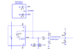
And I will make the conexion of the traco in the next way:

OpAmpScheme4.png

Greetings
 

Hi,

correct so far.

Does the ATSAME54P20A ADC have
* a differential mode sampling feature, or
* simultaneous sampling feature?

If so, then wire Sensor_0V to the ADC as additional channel / reference_channel.

Klaus
 

Hi again!

Thanks for the tip Klaus.

The uC ADC has the possibility to do differential sampling. However after reading the datasheet is not clear which are the "negatives" IO pins to carry out this sampling mode. It looks that there are 32 analogue inputs but you can only use 10 + 10 analogue inputs for the differential setup: AIN1P....AIN10P & AIN1N...AIN10N. However it results very tricky to identify in the datasheet the "positive" and the "negative" ADC pins of the uC. But in any case, the uC has not dedicated ADC IO pins. All the IOs of the uC are configurable and they can work as digital IOs too depending on the register configuration. Therefore Does it make sense to identify the negatives analogue ADC IOs
to connect them to 0V_Sensor? Or maybe it is better to configure the internal register of the ADC uC like single ended sampling mode and configure the theoretically negative ADC IOs like digital inputs IOs for example?

Furthermore the uC does not have an output pin vref/2 (or at least I did not find it in the IO pin section of the datasheet). So I need to modify the solution proposed in the previous messages having in mind the next two alternatives:

1) Provide to the input Vref IOs of the uC ADC a very stable Vref/2 reference (for example using the opamp + npn transistor + zener diode proposed previously)
2) The uC ADC uses it's internal Vref/2 reference and connect to 0V_Sensor a Vref/2 generated outside of the uC with the opamp + npn + zener diode proposed previously too.

What do you think is the best option? I like more the first alternative but I would like to hear other options.


Thanks for everything
Greetings
 

Status
Not open for further replies.

Similar threads

Part and Inventory Search

Welcome to EDABoard.com

Sponsor

Back
Top