Continue to Site

Welcome to EDAboard.com

Welcome to our site! EDAboard.com is an international Electronics Discussion Forum focused on EDA software, circuits, schematics, books, theory, papers, asic, pld, 8051, DSP, Network, RF, Analog Design, PCB, Service Manuals... and a whole lot more! To participate you need to register. Registration is free. Click here to register now.

Difference betweeen sooch biasing and wide swing biasing mirror

Status
Not open for further replies.

Junus2012

Advanced Member level 5
Joined
Jan 9, 2012
Messages
1,552
Helped
47
Reputation
98
Reaction score
53
Trophy points
1,328
Location
Italy
Activity points
15,235
Dear friends,

I am trying to use this circuit attached below for biasing the cascode transistors in of the Op-amp. This circuit was highlighted to me by Dominik but I still unable to understand the princible of operation regarding the voltages Vntail, Vncas1 and Vncas2.
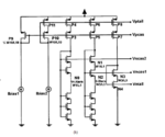

sooch_biasing circuit.PNG


What I know is that:

Vtail = Vov+Vth
Vncas1= 2Vov+Vth
Vncas2 = 3Vov+Vth

But I dont know how it is coming or the setting to generate these voltages from this circuit.

What will be the difference by biasing using the wideswing mirror, the one shown below

mirror.PNG

Thank you in advance

Best Regards
 

Dear friends,

I am trying to use this circuit attached below for biasing the cascode transistors in of the Op-amp. This circuit was highlighted to me by Dominik but I still unable to understand the princible of operation regarding the voltages Vntail, Vncas1 and Vncas2.


View attachment 159091


What I know is that:

Vtail = Vov+Vth
Vncas1= 2Vov+Vth
Vncas2 = 3Vov+Vth

But I dont know how it is coming or the setting to generate these voltages from this circuit.

What will be the difference by biasing using the wideswing mirror, the one shown below

View attachment 159092

Thank you in advance

Best Regards

Hello Suta,

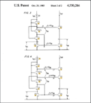
Could you please give me some information about the first scheme, it is not clear fro me even after the Sooch patent
 

What is it that's not clear?

thanks Suta,

how these voltages are generated

Vncas1= 2Vov+Vth
Vncas2 = 3Vov+Vth

- - - Updated - - -

why he multiplied N1 with 6 and No with 14 ?

- - - Updated - - -

also why transistors N2 is biased from No,, they can both be independent from each other
 

Desr Suta, you can also refer to this picture


sooch2.png
 

I think we discussed this kind of cascde biasing before.

https://www.edaboard.com/showthread...nt-mirror&highlight=sutapanaki+current+mirror

https://www.edaboard.com/showthread...nt-mirror&highlight=sutapanaki+current+mirror

the schematic above in your posts is not much different, just a stack of transistors.

The Sooch current mirror is totally different arrangement.

View attachment 159117

Thank you Suta for your reply

I think I was mistakenly calling the scheme as sooch after I read it from the author in post #1,
then it means I am interested on this,,,,, we discussed abot the stack but not about this one

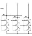
Let me please refer again to this circuit

soocheee.png

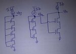
why transistors in VB2 branch is chained to the transistors in VB3 branch, I can make them work like this, what will be the difference in performance

New Doc 20.jpg
 

Yes, you can make them work like you showed. I don't know what the idea is behind the first circuit with the 3 branches. It just creates cascode voltages, the Vb3 higher than Vb2. I can only offer you a very approximate view point and that's kind of based on square law devices. For example for the branch of Vb3, we can assume that the bottom two transistors are in triode region and the top one in saturation. Also, we know that in triode, the Ron is approx equal to 1/gm of the same transistor if it was in saturation. This is approximate and for square law devices. SO, the bottom two transistors in triode are each 3x smaller, so together they form a Ron that is 6/gm and the voltage drop across that Ron is (6/gm)*IB=3*(2/gm/IB)=3*Vov. Thus the voltage at VD2 for the leftmost branch is 3*Vov. The top transistor in saturation will have Vgs= Vth+Vov and VB3=Vth+4*Vov, again very approximately. You can continue like this for the remaining two branches.
 

@Junus2012
Often it is hard to understand why the circuit, in your case a bias circuit, is constructed in this or that way, especially when the bias circuit is shown without all the other blocks. Sometimes you want one bias branch to be depended on the other one or you want one branch to turn on later that the other one. I would propose, that you try to use the bias branch that you understand and in case of problems or bad parameters try to optimize it or modify or change.
 
Status
Not open for further replies.

Part and Inventory Search

Welcome to EDABoard.com

Sponsor

Back
Top