Saraadib
Member level 4
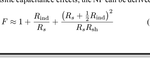
I mean, assume I build this circuit (This filter).
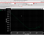
I use the probe station to measure the transfer function of this circuit. should I measure the S parameter of the circuit(Filter) to see transfer function?
I use the probe station to measure the transfer function of this circuit. should I measure the S parameter of the circuit(Filter) to see transfer function?
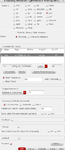
 arasitic ressistance of inductor and RS is :source resistance