Continue to Site

Welcome to EDAboard.com

Welcome to our site! EDAboard.com is an international Electronics Discussion Forum focused on EDA software, circuits, schematics, books, theory, papers, asic, pld, 8051, DSP, Network, RF, Analog Design, PCB, Service Manuals... and a whole lot more! To participate you need to register. Registration is free. Click here to register now.

UC3845 ETD29 transformer PWM signal

Status
Not open for further replies.

ivan_mateo

Member level 1
Joined
Feb 11, 2019
Messages
40
Helped
1
Reputation
2
Reaction score
2
Trophy points
8
Activity points
385
Hello everyone,

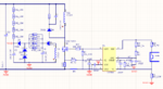
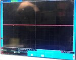
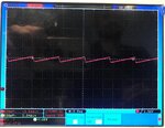
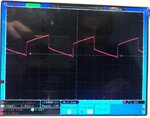
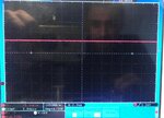
I design a simple flyback converter and assemby in PCB. My transformer etd29, primary indutance around 400uH and 40Turn, secondary is 9Turn. But when I drive UC3845 around 10V y applying external voltage from power supply not from line. There is some oscillaiton in PWM signal, as you can see in my attachment. Can anybody commet this issue? f=100kHz
Ekran Alıntısı.jpg
 

The problem with your simple flyback converter is we simply cannot see it. Please post a schematic and tell us where exactly the waveform is being checked.

Brian.
 

Before inserting transformer, the pwm signal is pure Square, but after transformer, it changed.
 

Attachments

  • Ekran Alıntısı.PNG
    Ekran Alıntısı.PNG
    78 KB · Views: 1,080
Last edited:

Hi,

Please show:
* the PCB layout
* the brand and exact type of R59 (datasheet)
* where at the PCB exactly you connected scope_GND and scope_signal

Klaus
 

Hi,

Please show:
* the PCB layout
* the brand and exact type of R59 (datasheet)
* where at the PCB exactly you connected scope_GND and scope_signal

Klaus
Ekran Alıntısı.PNG

R59 simple shunt resistor. It can be related transformer. Because I wound it by hand.
 

the fet might well be dead ...

- - - Updated - - -

or the transformer phasing or gap may be wrong ...
 
Hi,

You know you gave just half of the requested informations...
You will have your reasons....
Thus I can't verify the some items.

Anyway. Sadly you wasted almost one layer. The red layer is almost empty...why did you miss to make a ground plane?
Especially with switching power designs a solid ground plane is so important...

Klaus
 
A flyback transformer needs a gap in the core ( unless for VERY low power ) to store the energy, It is essentially a well coupled inductor.

With no gap the transformer will saturate ( Bpk ) and cause the supply volts to sag due to the large current through the Tx as a result ...

and the ckt will not work very well and you may kill your fet with overvolts at turn off ...

- - - Updated - - -

Also the DOT needs to go to pin 7, so that, at turn off, this pin rises positive and puts an impulse of current into the cap etc ...

- - - Updated - - -

yo may have to reconnect your Tx pins to achieve this.
 
I wound for flyback.
May be. You would want to correct the dot marking in schematic.

A flyback transformer needs a gap in the core
The numbers in post #1 suggest about 0.4 mm air gap, should be O.K.

It's unclear at which node the post #1 waveform has been picked up.
 

As Easy Peasy says you may well have blown the fet...and with a mains circuit and a blown fet...you may have blown the uc3845 too...a blown fet often goes short drain to gate...so your uc38xx may have snuffed it
Is the UC3845 still compus mentuis?
Does it give a 5V output...does the oscillator pin show the ramping waveform?
 
Hi,

PCB layout:

See the picture. I showed the current flow loop for the gate current.
A good layout: should have as low as possible enclosed loop area. (low EMI, EMC) And it should have all the return path of signals of one side on the GND_Plane at the other side.
So the loop area becomes close to zero and the loop inductance is minimized. I assume a good PCB layout will have about 1/100 of the loop inductance than your layout. (just guessing)
SMPS_Loop.PNG

And about R56: A metal strip is good, a wire wound not.

Klaus
 

Hi,

PCB layout:

See the picture. I showed the current flow loop for the gate current.
A good layout: should have as low as possible enclosed loop area. (low EMI, EMC) And it should have all the return path of signals of one side on the GND_Plane at the other side.
So the loop area becomes close to zero and the loop inductance is minimized. I assume a good PCB layout will have about 1/100 of the loop inductance than your layout. (just guessing)
View attachment 158466

And about R56: A metal strip is good, a wire wound not.

Klaus

I tried to minimize the drain current path, the high current path. Bulk cap, primary winding, mosfet drain to source and shunt resistor and gnd. I am confused about that if the gate current path is short, leakage inductance will be less. And if the Cds and leakage inductance are less, it will be less oscilation on gate signal. Also, most of source says that high current path have to be short. Which approach is more important? Because it can would not have possible everytime to do both of them.

- - - Updated - - -

I already have removed Mosfet and observed waveforms of IC. I attached photos Pin1, pin4, Pin6, Pin8 respectively.
pin1.jpg
pin4.jpg
pin6.jpg
pin8.jpg
 

Attachments

  • pin1.jpg
    pin1.jpg
    87.3 KB · Views: 87
  • pin4.jpg
    pin4.jpg
    87.9 KB · Views: 92
  • pin6.jpg
    pin6.jpg
    82 KB · Views: 76
  • pin8.jpg
    pin8.jpg
    87.7 KB · Views: 89
Last edited:

The pin 6 waveform seems to indicate a defective or wrongly calibrated oscilloscope probe.
 
The pin 6 waveform seems to indicate a defective or wrongly calibrated oscilloscope probe.

Thank you. Yes, you are right. When I changed the probe, the problem was solved. But I could not comment the previous waveform, it was very different.
pin6.jpg
 

The post #1 waveform has apparently similar problems. Repeat the measurement with verified probe.
 
The post #1 waveform has apparently similar problems. Repeat the measurement with verified probe.

Ok. I will try it without removing the transformer.
 

Hi,

I tried to minimize the drain current path, the high current path. Bulk cap, primary winding, mosfet drain to source and shunt resistor and gnd.
You know: No signal goes one way, it always needs a return path. And if the return path is long and high impedance the whole signal will be slow and ringing.
--> Don´t see only the signal from A to B, but also the (HF) path back from B to A.

I am confused about that if the gate current path is short, leakage inductance will be less. And if the Cds and leakage inductance are less, it will be less oscilation on gate signal.
The phrase "leakage" inductance often is used with transformers. I didn´t use this phrase. So I´m not sure whether you talk about the inductance on the PCB or the transformer.
In either case it should be low.
--> here a Ground plane brings a benefit, because the returning current shares the opposite side of the original current path. The current is reversed, the magnetic field is reversed and thus the magnetic field compensates... resulting in way less overall inductance. (and EMI)

Also, most of source says that high current path have to be short. Which approach is more important? Because it can would not have possible everytime to do both of them.
True, the power path is important. But rining often happens because both signals (power and gate) share the same (return) path: from source via shunt to bulk capacitor.

When the controller wants to switch ON, then it rises the gate drive signal (with respect to the driver IC GND)..Then the mosfet becomes conductive, current begins to flow .... through shunt to bulk capacitor .... any inductance in this path will lift the voltage on the MOSFET´s source ... reducing V_GS (since the driver IC GND - and thus the gate_drive_voltage - is not lifted the same ammount than the source voltage). .. --> this is the feedback with it´s phase shift, that enables ringing. (the driver IC wants to increase V_GS where the source path inductance tries to lower V_GS).

This (hopefully) answers "which approach is more important?" --> both are important.
But since the power path carries higher current it will cause higher voltage drop on the common path. But don´t underestimate the gate drive current. It may be several amperes, depending on circuit..

****
You refer to (...most of source says...) documents about SMPS. If they are modern ones from reliable sources like MOSFET manufacturers, SMPS controller manufacturers, universities.. don´t they all recommend a solid GND_plane, low impedance shunt resistors, return paths, suitable voltage reference points...? In my eyes they should...


Klaus
 
Status
Not open for further replies.

Similar threads

Part and Inventory Search

Welcome to EDABoard.com

Sponsor

Back
Top