Continue to Site

Welcome to EDAboard.com

Welcome to our site! EDAboard.com is an international Electronics Discussion Forum focused on EDA software, circuits, schematics, books, theory, papers, asic, pld, 8051, DSP, Network, RF, Analog Design, PCB, Service Manuals... and a whole lot more! To participate you need to register. Registration is free. Click here to register now.

[SOLVED] SMA-Microstrip transition removal for large-signal measurement of PA

Status
Not open for further replies.

ueckid

Member level 1
Joined
Mar 22, 2017
Messages
39
Helped
2
Reputation
4
Reaction score
3
Trophy points
1,288
Location
Osaka, Japan
Activity points
1,692
Hi all,

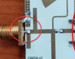
Could anyone please tell me how to remove SMA connector-Microstrip transition for large-signal measurement of a PA? In measurement, I noticed that this transition will shift the optimum load impedance seen by Transistor and therefore degrading the output power, gain and efficiency of my PA designed at 2.4 GHz. In measurement the measured power is lower than simulation by about 3 dB.

Please see figure below.

I wonder how I can tune load/source impedance in practice to compensate this impedance shift?

Large_Signal.jpg
 

Try to make a better (shorter) connection from SMA ground to the PCB ground. At the moment, you have a bit too much path length there. Parasitic ground path inductance is as bad as signal path inductance.
 
  • Like
Reactions: ueckid

    ueckid

    Points: 2
    Helpful Answer Positive Rating
Try to make a better (shorter) connection from SMA ground to the PCB ground. At the moment, you have a bit too much path length there. Parasitic ground path inductance is as bad as signal path inductance.

Thanks for your valuable advice, I will try to follow your guidance.
Then for the parasitic signal path inductance, how can we eliminate it?
 

Then for the parasitic signal path inductance, how can we eliminate it?

Short and direct connection from connector ground to microstrip (backside) ground. Your ground path with these connector (not designed for this side mounting) has too much length in the photo.


A while ago I had shown here that gaps in the ground, with some longer ground path through such SMA ground pins, results in poor S11 at high frequency. However, that trouble was at higher frequency, and 2.4GHz was not that bad.

coax5_gaps.PNG

coax6_gaps.PNG

coax4.PNG

coax1.PNG
 
It happen to have in my EM simulator a circuit very similar to the presented one, on the same frequency.
Replicating the PCB transition that you have was almost impossible to get the 3dB loss that you mention (I got just 0.2dB)
Most probably my circuit use a different PA, but shouldn't be such difference. You may check for other issues, not only for this transition.
Those long wires and components on the bias networks, looks ridiculous for a 2.4GHz circuit.
For these bias circuits, use SMD capacitors with SRF at 2.4GHz (let's say a GQM1875G2E120JB12 from Murata), and low ESR electrolytic capacitors (tantalum).
 
  • Like
Reactions: ueckid

    ueckid

    Points: 2
    Helpful Answer Positive Rating
Short and direct connection from connector ground to microstrip (backside) ground. Your ground path with these connector (not designed for this side mounting) has too much length in the photo.


A while ago I had shown here that gaps in the ground, with some longer ground path through such SMA ground pins, results in poor S11 at high frequency. However, that trouble was at higher frequency, and 2.4GHz was not that bad.

View attachment 158320

View attachment 158321

View attachment 158322

View attachment 158323

Thanks for additional information.
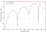
In my situation, deviation in magnitude between EM Sim. and Meas. is not so significant at low frequencies including 2.4 GHz as attached pictures.
It becomes large at high frequencies as you indicated.

However, as you can see in my attached pictures, phase of S-parameters between Sim. and Meas. deviate even in low frequencies due to some unintentional extra transmission lines somewhere. This leads to deviation of optimum load and source impedances seen by Transistor degrading large-signal performance including output power, gain and efficiency.

Slide1.JPG
Slide2.JPG

- - - Updated - - -

It happen to have in my EM simulator a circuit very similar to the presented one, on the same frequency.
Replicating the PCB transition that you have was almost impossible to get the 3dB loss that you mention (I got just 0.2dB)
Most probably my circuit use a different PA, but shouldn't be such difference. You may check for other issues, not only for this transition.
Those long wires and components on the bias networks, looks ridiculous for a 2.4GHz circuit.
For these bias circuits, use SMD capacitors with SRF at 2.4GHz (let's say a GQM1875G2E120JB12 from Murata), and low ESR electrolytic capacitors (tantalum).

Thanks for your recommendations. First I also thought that the loss is caused by the bias circuit. But you can see results of S-parameter measurement of my PA, the difference between Sim. and Meas. at low frequency is not significant. I think the bias network has been designed well. For RF short, a radial stub was used at one end of a lamda/4 line. I have evaluated this bias circuit in EM simulation.

I also noticed that there is a remarkable deviation between drain current as attachment. Is this caused by deviation in output power?

Slide1.JPG
Slide2.JPG
Ids.jpg
 

You didn't show the bottom side of the PCB, hence we can't know how good or bad the transition is. The connector shown in post #1 is a dedicated card edge receptacle as far as I see, but I don't know if the substrate height is matched.

Comparing simulation with measurement, how do you know that it's not the transistor causing the major deviation?

Your objectives are partly unclear. With an amplifier exposing positive gain only below 3 GHz, what's the purpose of having exact measurements up to 10 GHz?

The strongest deviation is seen in S12. Beside possible crosstalk around the PCB, we would expect the transistor and it's mounting as primary source of bad S12.
 
  • Like
Reactions: ueckid

    ueckid

    Points: 2
    Helpful Answer Positive Rating
However, as you can see in my attached pictures, phase of S-parameters between Sim. and Meas. deviate even in low frequencies due to some unintentional extra transmission lines somewhere. This leads to deviation of optimum load and source impedances seen by Transistor degrading large-signal performance including output power, gain and efficiency.

I don't get your point here - you seem to have 50 Ohm lines with 50 Ohm source/load, so the extra length will not change impedances seen by the DUT.
 

The OP is looking at Sxx phase in the first place, which is actually meaningless.
 

You didn't show the bottom side of the PCB, hence we can't know how good or bad the transition is. The connector shown in post #1 is a dedicated card edge receptacle as far as I see, but I don't know if the substrate height is matched.

Comparing simulation with measurement, how do you know that it's not the transistor causing the major deviation?

Your objectives are partly unclear. With an amplifier exposing positive gain only below 3 GHz, what's the purpose of having exact measurements up to 10 GHz?

The strongest deviation is seen in S12. Beside possible crosstalk around the PCB, we would expect the transistor and it's mounting as primary source of bad S12.

Thanks for your kind suggestions.
I will post backside of my PCB later. Actually, since the substrate height is just 0.75 mm, I used a buffer aluminum plate on the backside for soldering the SMA ground edge mount to ground PCB.
The transistor should cause the deviation but I don't know how to verify this issue in measurement?
I am measuring the PA at 2.4 GHz and I just would like to check performance at this freq point not 10 GHz.
I will check if the issue is device mounting in measurement and thanks a gain for this nice suggestion.

- - - Updated - - -

I don't get your point here - you seem to have 50 Ohm lines with 50 Ohm source/load, so the extra length will not change impedances seen by the DUT.

I am just wondering that if the transition makes external 50 Ohm to a different impedance?

In measurement of the output matching circuit, if I used port extension technique in VNA, measured impedances at f0, 2f0 and 3f0 agree well with EM Sim. but w/o using the port-extension, there was significant deviation of these impedances between Meas. and EM Sim. Or we can see a phase shift (clockwise rotation) of these impedances on the Smith chart.

This makes me think that the issue is due to some phase shift somewhere in the PCB or crosstalk in PCB.

Impedances.jpg
 

I think we're discussing different aspects here. Phase shift doesn't always mean change of impedance.

The impedance measured into the amp - as seen from the load side - moves around the Smith chart when you add line length in between. But the impedance seen from the amp into a 50 Ohm load remains 50 Ohm, no matter how much 50 Ohm line length you add in between.
 
  • Like
Reactions: ueckid

    ueckid

    Points: 2
    Helpful Answer Positive Rating
I think the bias network has been designed well. For RF short, a radial stub was used at one end of a lamda/4 line. I have evaluated this bias circuit in EM simulation.

Sorry that I have to insist, you may design and simulate well the bias circuit, but the practical implementation you did is wrong.

Practical implementation of the decoupling bias network has a huge impact on the performances of this kind of PAs:
**broken link removed**
 
  • Like
Reactions: ueckid

    ueckid

    Points: 2
    Helpful Answer Positive Rating
Sorry that I have to insist, you may design and simulate well the bias circuit, but the practical implementation you did is wrong.

I also don't understand your concern. The large "non-RF-style" elements behind the radial stub are on the DC-side of things.
 

I think we're discussing different aspects here. Phase shift doesn't always mean change of impedance.

The impedance measured into the amp - as seen from the load side - moves around the Smith chart when you add line length in between. But the impedance seen from the amp into a 50 Ohm load remains 50 Ohm, no matter how much 50 Ohm line length you add in between.

I understood that 50 Ohm will not change no matter 50 Ohm line length added. However, do you think that the transition is not an uniform lines with 50 Ohm?

As you can see in my measurement of the output matching circuit, when I used port-extension technique in VNA to compensate the phase shift somewhere (shown on Smith chart), the simulated impedances became close to the measured ones. So I think there should be a phase shift somewhere (may be the transition?).

Impedances.jpg

- - - Updated - - -

Sorry that I have to insist, you may design and simulate well the bias circuit, but the practical implementation you did is wrong.

Practical implementation of the decoupling bias network has a huge impact on the performances of this kind of PAs:
**broken link removed**

I am sorry I don't really get your point, Do you mean a lamda/4 terminated with a radial stub at one end is not practical?

- - - Updated - - -

I also don't understand your concern. The large "non-RF-style" elements behind the radial stub are on the DC-side of things.

Do you mean the ground area which is near the radial stub?
 

I am sorry I don't really get your point, Do you mean a lamda/4 terminated with a radial stub at one end is not practical?

Lamda/4 terminated with a radial stub at one end IT IS practical, but what you have in your real PCB board is NOT practical. Follow what is written in the link I posted and you will get good results.
Use only SMD passive components, with the right values.

From an EM simulation on a similar circuit, the small layout mismatch that you have on the output SMA connector is not giving 3dB extra loss.
But a small decoupling mistake on the bias lines would give what you get (loss in power, less linearity, less DC efficiency, etc.)
 
  • Like
Reactions: ueckid

    ueckid

    Points: 2
    Helpful Answer Positive Rating
Lamda/4 terminated with a radial stub at one end IT IS practical, but what you have in your real PCB board is NOT practical. Follow what is written in the link I posted and you will get good results.
Use only SMD passive components, with the right values.

From an EM simulation on a similar circuit, the small layout mismatch that you have on the output SMA connector is not giving 3dB extra loss.
But a small decoupling mistake on the bias lines would give what you get (loss in power, less linearity, less DC efficiency, etc.)

Thank you. Do you mean I should try a combination of a RF-bypass capacitor with a RF-choke inductor using SMD components?

Anyway, I will try bias methods in the literature you posted to check if the issue caused by bias circuit.

I forgot to mention one more important thing, when I made a large-signal simulations in ADS using a large-signal model of transistor combining with measured S-parameters of input matching circuit and output matching circuit, I noticed that if I didn't use the port-extension technique in measurement of IMN and OMN, output power was degraded by around 3 dB as indicated in the whole PCB measurement. However when I used port-extension in measured S-parameters of the IMN and OMN to get better optimum impedances compared with Sim. all large-signal results (PAE, Gain, Pout) looked good.
 

Getting the reference planes is of course very important, so careful port extension might be required, depending on your port calibration method.

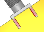
But what is also required is careful connection, you have introduced so much parasitic inductance in your coax-to-PCB transition that I would not trust your measurements. Looking at your photo, that is a several nH parasitic series L due to the gap and the long ground path.

ser_ind.png

What does the backside soldering look like?
 
  • Like
Reactions: ueckid

    ueckid

    Points: 2
    Helpful Answer Positive Rating
But what is also required is careful connection, you have introduced so much parasitic inductance in your coax-to-PCB transition that I would not trust your measurements. Looking at your photo, that is a several nH parasitic series L due to the gap and the long ground path.

What does the backside soldering look like?[/QUOTE]

Thanks, I think this is actually the issue I am trying to figure out. Do you think if this parasitic inductance is really serious at 2.4 GHz for degradation of large-signal performance of PA?

I am sorry I don't have an available pic of backside PCB right now, I will post it later. But the backside of the SMA connector has a longer ground path than the front side, then I think this adds more parasitic inductance to my PCB as you indicated. But once again, is it really serious at 2.4 GHz?
 

Your test board is not so good at all..Ground connections are extremely sensitive at RF frequencies and its' GND connections are very poor.
Find a polished aluminum mass and make the connectors' GND screws are tightly screwed to this mass and GND layer touches very well to this base aluminum.
Find a high quality "PCB Type SMA Receptacle " from distributors with thin center connectors like this..
https://www.mouser.fr/ProductDetail...f%2BEuFsOrvkNvxXAl2ZL6rgRRI3Bis0vZG27s1Utiw==

Any better alternative can also be found, no doubt.But you SMA connector is not very appropriate for SMD applications.
But GND GND GND.. this is important.
 
Last edited:
  • Like
Reactions: ueckid

    ueckid

    Points: 2
    Helpful Answer Positive Rating
A correctly mounted SMA PCB edge connector isn't that bad. The presented photos however show an excessive gap and the second PCB in post #14 has a ground pin cut. We didn't yet see if the bottom side has the expected continuous ground.

A simulation can show if the imperfect connector mount allone is sufficient to cause a 3 dB gain drop. I would rather guess that's due to a combination of several design details.
 
  • Like
Reactions: ueckid

    ueckid

    Points: 2
    Helpful Answer Positive Rating
Status
Not open for further replies.

Part and Inventory Search

Welcome to EDABoard.com

Sponsor

Back
Top