Continue to Site

Welcome to EDAboard.com

Welcome to our site! EDAboard.com is an international Electronics Discussion Forum focused on EDA software, circuits, schematics, books, theory, papers, asic, pld, 8051, DSP, Network, RF, Analog Design, PCB, Service Manuals... and a whole lot more! To participate you need to register. Registration is free. Click here to register now.

adding reset function to D Flip FLOP

Status
Not open for further replies.

yefj

Advanced Member level 4
Joined
Sep 12, 2019
Messages
1,176
Helped
1
Reputation
2
Reaction score
3
Trophy points
38
Activity points
7,069
adding reset function to D Flip FLOP for phase detector

Hello, I have designed a rising edge D-flipflop as shown bellow using CML method.
I could have just connect the output to NMOS switch and discharge it to ground.
However in our reset signal comes at Q, so basickly if we have Q=1 then this Q=1 is used to turn Q into Q=0.
so we have oscilation.

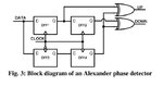
How do i add "reset" to my D-flip flop So i could use it in phase detector as shown bellow?
Thanks.
1.JPG
2.JPG
3.JPG
 
Last edited:

I don't recognize an edge sensitive DFF, it's a level sensitive latch. You need to connect two of it in a master-slave structure and feed the reset to both stages.
 

Hello, i have painted on the clock signal the rising edges and we see that output Q changes as clock rises.
could you please show on the signal photo why its not edge triggered?

Thanks
 

Supplement the diagram with an D input changing during CLK high, e.g. shift the falling edge from 2.0 ns to 1.5 ns and you'll see that it's not edge triggered.
 

Yes, i saw that its level Triggerd not edge triggered,i will fix that.
Regarding my reset issue:
Our reset signal comes from the FLIP FLOP it self,so there is a problem where in certain case as Q gets high we get in the phase detector AND gate of both Q
and the FLIP FLOP recieves RESET=1 and at once it has to turn Q=0,
there is a problem in hear because the Q=1 signal basickly has to create RESET=1 which immidiatly turns Q=0
so there is an oscliation problem.If our reset signal was external then it was no proble , but here its self generating.
How do i implement RESET for this CML flip flop configuration for phase detector use?
Thanks.
4.JPG
 

There's no general "oscillation" problem with a proper DFF, but it may be a problem related to reset input hold time. If the required hold time is larger than the R to Q propagation delay, than the output waveform is unpredictable and may be even oscillating.

You know, that this phase detector topology is often discussed in literature, e.g. by Razavi. I'd assume that it's least working with the DFF designs used therein.

Did you re-check with the the master-slave structure, resetting both master and slave output signal?
 

I managed to create a D-FLIP FLOP as shown bellow.
The question remains is how to insert in the following diagram the reset functionality?
connecting the Q output to ground VIA NMOS (where reset connected to gate)is not the best idea.
What reset is used for phase detector?
Thanks.

1.JPG
2.JPG
3.JPG
 
Last edited:

Im sure CML FF with reset is discussed in literature. I had an idea how to implement it, but I'm not regularly working with CML and don't want to suggest my reinvented square wheel.
 

Hello, I am trying to implement the following phase detector shown bellow with my CML flip flop, it samples 4 times the data and somehow shows if CLK lags behind the data.
I cant see the last part,The difference between the upper sampling and lower is theat the lower samples at first with falling edge.
Another thing is Why for UP it uses 1,3 DATA but for down it uses 2,3 DATA
What is the logic in that?
Thanks.

https://ieeexplore.ieee.org/stamp/stamp.jsp?tp=&arnumber=4149052
6.JPG
5.JPG
 

Attachments

  • 4.JPG
    4.JPG
    34.1 KB · Views: 186

Hello, I am trying to implement the following phase detector shown bellow with my CML flip flop, it samples 4 times the data and somehow shows if CLK lags behind the data.
I cant see the last part,The difference between the upper sampling and lower is theat the lower samples at first with falling edge.
Another thing is Why for UP it uses 1,3 DATA but for down it uses 2,3 DATA
What is the logic in that?

The clock input is inverted on the lower left DFF (DFF3).
Three samples are used, taken with a half clock cycle interval between the samples.
With your numbering, no 2 is the oldest sample, no 3 is the middle and no 1 is the newest.
It is logical to compare with the middle sample, so no 3 is used for both UP and DOWN.
 

(1) is one clock cycle delay (2) is two clocks delay so (3) i assume is 1.5 cycles delay.
Why a data sampled falling edge with respect to data of high edge sampling is half cycle delay?
Thanks?

Hello, I am trying to implement the following phase detector shown bellow with my CML flip flop, it samples 4 times the data and somehow shows if CLK lags behind the data.
I cant see the last part,The difference between the upper sampling and lower is theat the lower samples at first with falling edge.
Another thing is Why for UP it uses 1,3 DATA but for down it uses 2,3 DATA
What is the logic in that?
Thanks.

https://ieeexplore.ieee.org/stamp/stamp.jsp?tp=&arnumber=4149052
View attachment 158301
View attachment 158300
 

Hello, have tried to implement half clock dlay by inverting the clock on my CML.
but there is no shift of signal i get unuque signal from each output.
Where did i go wrong?
Thanks.

1.JPG
2.JPG
 

Status
Not open for further replies.

Part and Inventory Search

Welcome to EDABoard.com

Sponsor

Back
Top