Continue to Site

Welcome to EDAboard.com

Welcome to our site! EDAboard.com is an international Electronics Discussion Forum focused on EDA software, circuits, schematics, books, theory, papers, asic, pld, 8051, DSP, Network, RF, Analog Design, PCB, Service Manuals... and a whole lot more! To participate you need to register. Registration is free. Click here to register now.

Question why one of the MOSFET burn shorted in my SS relay

Status
Not open for further replies.

Alan8947

Full Member level 4
Joined
Sep 21, 2016
Messages
215
Helped
9
Reputation
18
Reaction score
11
Trophy points
1,298
Activity points
3,746
Hi

I have one MOSFET failure with S shorted to D and G is 10ohm to S and D. Attached is the schematics, (A) is the original circuit. I use this as SS relay at the output of the hifi power amp, as shown, I use 6 MOSFET to lower the Rdson. The MOSFETs are driven by an opto coupler ASSR-V621 with data sheet:

https://www.digikey.com/product-detail/en/broadcom-limited/ASSR-V621-002E/516-2961-ND/2211292

Let me be specific, I have been using the circuit in a few amps in the pass 4 years, this is the FIRST time one failed. BUT I am paranoid as I designed MOSFET power circuit before and only time I've seen failure like this is oscillation ( local around the MOSFET). MOSFET are usually very rugged. So one failure is alarming to me.

I know it's very common to use a resistor in series with each gate to make the impedance +ve to avoid oscillation, but this circuit is a little different. All the SMPS have low output impedance driver to drive the MOSFET, so gate resistor easily avoid any oscillation. BUT if you look at the datasheet of the ASSR-V621, the drive to the gate of the MOSFET is a photo diode that behave like a current source with very high output impedance, I am not sure it will work even if I put 6 individual resistors on each gate of each MOSFET as shown in circuit (B).
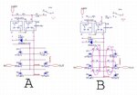
SS relay.JPG
I want to hear opinion on how to better protect the MOSFET from potential oscillation.

Thanks

Alan

- - - Updated - - -

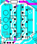
I want to show the layout of the pcb, I did my best to layout with RF in mind as much as possible, I have to use TO-220 as the SMD takes up too much room. You can see I use copper planes as much as possible, there are no long traces running around. Only the gates are connected with traces, all the D and S are connected by copper planes.
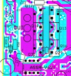
SS relay layout.JPG
 

Hi,

Electronic parts may be killed by:
* overvoltage
* overcurrent
* overtemperature (caused by too high power dissipation. For short or long time)

Your design should avoid all these situations.

We can only guess, because you don't give any of the above mentioned values.
My idea:
There is no overvoltage protection. Not against unexpected ESD, nor against expectable overvoltage caused when switching off (inductive) load.
Any tiny piece of time (microseconds or even less) where the voltage across the Mosets is above the specified "absolute maximum rated voltage) may harm the internal isolation barrier. Mistreating the isolation barrier may cause immediate failure, but it may also cause long time failure. Maybe after years.

So any ESD pulse during production, packaging, transport, installation, handling ... may be the root cause of a long time failure.
As said above, audio speakers include a coil (inductance), crossover with a coil and even the wiring may act as inductance.
Thus it's quite expectable that during switch OFF a high voltage pulse will be generated.
--> install a fast overvoltage protection.

Now modern audio amplifier often are class D (or other HF switching). Maybe this also can cause problems.

Klaus
 

Hi Klaus

Thanks for you reply. The failure happened when I was not driving speakers, just a test load. I usually have clamping diode to ensure voltage never even close to the Vdsmax. I did forgot to put in the diode in my test setup. That's the first thing I thought about.

I ruled over voltage out because it is on bench test, I use a 4ohm metal film resistor as load driving through a 3ft thick speaker cable. There should be no inductance to speak of. The speaker cable is made of multi insulated 16 gauge cables twisted together to ensure low series inductance. So I don't think inductance kick is the problem. BUT I have to say, I did forgot to put in the clamping diode on the +ve side.

After I posted the thread, I actually build the switch alone and look at the signal on the scope across the S and G. I drove with a square wave about 5Hz and look at the scope, the signal looked very clean, no ringing of any sort. But of cause, it's hard to catch a burst of oscillation like this.

If you have an opinion on this, let me know

Thanks
 

You didn't tell, but I guess the MOSFET was killed during a switch-off test? If so, what was the load current?

Besides overvoltage caused by load inductance, I would also consider SOA exceedance due to slow switching. With the large Cgs amount, turn off is extended to > 1 ms. Oscillations may occur during turn off, but only transitional as a side effect of slow switching. Due to threshold voltage variations, you should expect that worst case one transistor has to absorb the total switching energy.
 
Hi FvM

You might be onto something. It's too late to take pictures of the driving signal of the ASSR-V621 to the G. The turn on time is very slow, the turn off time is actually very fast as it has a turn off circuit built in. But your concern of one pair of the three turn on first and take on the whole load will be the same as turn off as you describe. That is one pair might turn on first and take on the whole load current.

I don't know exactly what I did that burn the MOSFET, but I was doing stability test on the amp by putting a 24,000pF cap directly across the output of the pcb. That is the cap only goes through about 3inches of heavy wire ( 4 16 gauge wire in parallel) to the pcb. There is almost no series inductance to isolate the capacitor from the amp. I was testing for oscillation with clipping signal that swing +/-32V. So the surge of current through the capacitors might be very high as I have no inductance to tame the current spike down,

I was not switching the MOSFET on and off for testing. When the waveform was clipped so bad that it deform and produced DC that triggered the DC sensing circuit and shut off the MOSFETs. It just trigger here and there and I notice I lost the output after a while.

I did test also with over 100KHz clipping signal also, I can imagine the peak current is very high.

BTW, the 24,000pF is using 7 of the 3,300pF ceramic capacitor in parallel, so the loss and lead inductance is low, that make the peak current even higher. This might be the problem.

I looked at the waveform, the turn on time is very slow. I can speed it up by decrease R4 by half and speed up the rise time by a lot, maybe that will help. I'll take a picture of the waveform tomorrow.

Thanks and good night.

alan
 

What's the output stage power supply during the test? Does the amplifier implement instantaneous current limiting?
 

you say you use this circuit without fault for 4 years...and now a fet blows.......i reckon this is ESD problem...FETs are incredibly sensitive to ESD......i have worked in places that when PCBs with fets on them were reworked...even with esd mat and wrist strap being worn.....5% of the reworked boards would blow up....there is only one answer, and that is to handle fets as little as possible.
Some fets , from their manufacture , are more sensitive than others...the gate structure is microscopic, and impossible to make to great precision in every case...show a pic of your esd measures.

I have seen esd plugs going in to sockets where there was no earth in the socket!
 
What's the output stage power supply during the test? Does the amplifier implement instantaneous current limiting?

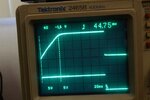
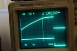
Here is picture of the waveform of the Gate signal ( across G-S), The rise time is about 100mS.

SS relay drive slow.JPG

I reduce R4 from 5.1K to 2.5K ( parallel another one on top) and this is the waveform. Notice it's a lot faster. Rise time is about 50mS.

SS relay drive fast.JPG

The fall time is like 10uS, very fast. Turn off is NOT an issue.


Regarding to current limit, there is NO current limit. In fact, I use 9 pair of big output transistors and run total of 1A bias current to ensure output impedance is very very low. The rail voltage is +/-32V. Instantaneous current is very high, must be over 100A as I have huge capacitor on the power supply in parallel with 10uF and 0.1uF for each and every power transistor. All for provide huge instantaneous current.

Like I said, it failed when I was testing with 24,000pF low loss capacitor right at the output of the pcb. That is like a shoot circuit with high frequency. I can imagine 100s of amps surge.

- - - Updated - - -

you say you use this circuit without fault for 4 years...and now a fet blows.......i reckon this is ESD problem...FETs are incredibly sensitive to ESD......i have worked in places that when PCBs with fets on them were reworked...even with esd mat and wrist strap being worn.....5% of the reworked boards would blow up....there is only one answer, and that is to handle fets as little as possible.
Some fets , from their manufacture , are more sensitive than others...the gate structure is microscopic, and impossible to make to great precision in every case...show a pic of your esd measures.

I have seen esd plugs going in to sockets where there was no earth in the socket!

Ha ha, I am embarrassed to say I recycle MOSFET on this protoboard. I use new ones in the real amplifier boards, but this is a prototype for testing only. BUT I was very careful, I TIED the G to S on each of the MOSFET before I desolder them from the old circuit boards. I use a grounded foam met on the bench and I double checked the soldering iron tip was grounded, I grounded myself before doing anything. After I removed the MOSFET from the old board, I still kept the jumper between the G and S and solder onto the new board before I remove the jumper. I think I did it as safe as human can already.

I know in the older days when I was using those CMOS 4000 series logic chips, they were very fragile, every time I probed the pins, they died eventually. But I thought these are big transistors with very high Cgs, it will take time to charge up and if I shorted the G and S before doing anything, I only remove the short after I soldered onto the new board, I should not have given a chance for the gate to charge up and blow the oxide. But of cause I could be wrong.

Is there anything I missed with this procedure that can blow the MOSFET?

Thanks

PS: I am born cheap, each of those transistor is like $5 and I use 6 of them each board!!! LOL!!!:-D
 

OK - assuming there is not enough peak current to destroy the mosfets - that leaves 2, 3 things - 1:- over voltage at turn off with enough ckt current to melt the die at turn off,

or,

2:- not enough heatsinking - the current is overheating the mosfets and the weakest one fails first, or,

3:- some times there is too much current - again killing the weakest one first.

Thanks for the reply, I tend not to think this is a problem. Rdson is 0.005ohm max if not lower depending on what transistor. Even if you calculate 50A continuous current, that's only going to be 0.25W of power on the transistor. I don't use heatsink, it's never even warm.

Thanks
 

New question


So nobody think it is a MOSFET oscillation?

- - - Updated - - -

I definitely going to speed up the rising edge by reducing R4 to 2.5K. But should I add a say 510ohm resistor in series with each of the G. It will make in messy doing the modification.....Or have to re-layout a new pcb.
 

Hi,

Even if you calculate 50A continuous current, that's only going to be 0.25W of power
This is only true, when the Mosfet is fully switched ON.
But during rising and falling of V_GS the R_DS_ON generates a lot more heat.

Klaus
 

show the Vds at turn off please ....

It is an analog switch ( SS relay), the signal is from +32V to -32V. The MOSFET used is Vds=100Vmax, so when it turns off, the output(load side) is being pull to the ground(0V) by the load resistor. So The max Vds is only 32V.

I am just covering all bases, I am going to speed up the rise time of the turn on signal, I am working on modifying the board to put a 220ohm resistor in series of each of the G of the 6 MOSFET. I had experience in the pass when a MOSFET self oscillate and burn, it goes very quiet, no smoke,no fire, it just die quietly like this failure. The symptom is all shorted out between all legs.

Actually I worked with a lot of high voltage pulsing circuits using MOSFET, my experience is when the Vds exceed the max, it just goes to zener and start drawing current, as long as it's within the dissipation limit, I have not seen one burn yet. This means it's NOT like as if the moment the Vds exceed the max spec., it just smoke and die or damage.

I designed a 1000V pulsing circuit with HV NMOS that is spec for 1000V. We were using it at the max 100% of the time, I don't know of a single failure in our system for years. Those MOSFET is very very rugged, only time I saw they die is if they oscillate and just die instantaneously and quietly with no fan fair. When they are over stressed, they usually die with noise and smoke, not quiet like this. That's why I am still thinking of oscillation.

I worked on a very high power constant current custom power supply that kept blowing the huge MOSFET, they are the chassis mount really big ones. Our problem was it just die, quietly, no fan fair. I fixed the oscillation and it never fail anymore. That's why I am so alarmed by the failure this time, I did not even know it failed until a day or two when I checked there's no output. ( I usually put the probe before the MOSFET switch, meaning I did not know the output is not going out!!!).
Thanks
 

Hi,

several times you wrote about no (or low) inductance.

My opinion:
* "No inductance" does not exist.
* when there is inductance, then you have to expect higher voltage (higher than 32V)
* I don't expect "self oscillation" without inductance. So if you experienced self oscillation, then you experienced inductance. And if the inductance killed a Mosfet in the past ...
* large cross section does not reduce inductance (significantly)
* stranded wires do not reduce inductance (significantly)

***
You talk about switching speed. From the schematic and datasheet informations I expect way higher switching times. Especially at switching OFF. Did you do a true V_GS measurement to verify your values?
Higher switching times will reduce the voltage generated by an inductivity, but it may violate SOA specification. (Don't expect equal distribution of dissipated power over n Mosfets)

Klaus

I should say "very LOW" inductance. If you look at the picture below, the S of all 6 transistors are connected to a copper plane as shown in light blue, I have a copper plane on the bottom layer that doesn't show here. The inductance of the plane should be very low. You can see the G of the 6 transistors are connected by traces, but it's as short as it can be already. You can see the D of the transistors are connected to a plane also.
SS relay layout2.JPG

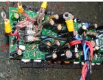
I also show a real picture of the stuffed pcb:

SS relay picture.JPG

You can see I use multiple wires to connect to the load, they are about 3inches long, both the + and - labeled in the picture are 6X16gauge wires to lower the wire inductance. The concept is like liptz wire in radio. If you look at the wire inductance, the series inductance different between a 10gauge and a 16 gauge wire is not that big a difference, so using one big wire is much inferior than use multiple smaller wires to lower the wire inductance.

So I am doing the best I can in lowering inductance from plane to MOSFET to plane to 3" multi-wires connection.

One thing I cannot help is the lead inductance of the TO-220 and the short trace from the ASSR-V621 to the 6 gates, I already minimize the length, but it's still like 1" or so. I think the main thing is the 6 gates are connected together and there might be interaction between the transistors. I am planning to put a series resistor like 100ohm right at the gate to isolate the gates of all the transistors and from the longer trace from the ASSR-V621.


Now, I am not saying this is the case, I am guessing as I said in the first post. I am hoping to have other points of views. Like the slow rising edge can run into problem of partially turn on with higher Rdson and might run into SOA problem. I am speeding up the rising edge for sure.

Thanks

- - - Updated - - -

Hi,


This is only true, when the Mosfet is fully switched ON.
But during rising and falling of V_GS the R_DS_ON generates a lot more heat.

Klaus

Yes, I realize the problem pointed out by FvM, and I reduce the R4 by half and you can see in the pictures in post #8 that I reduce the rise time by about half. Do you know of any other opto coupler that is faster than this. I only found ASSR-V621. I cannot reduce R4 any further as I am already pass the recommended current.

Thanks

- - - Updated - - -

Actually, let me ask


Whether anyone has a better solid state relay circuit? I need the on resistance as low as possible, like 0.002ohm or better, I need it to swing +/-40V analog signal from DC to at least 500KHz, and support high current.
 
Last edited:

Hi,

The inductance of the plane should be very low.
No. The resistance is low. Resistance depends on copper width, copper thickness and an length.

But impedance takes inductive impedance into account... and inductive impedance does not (much) care about copper thickness and copper width.

Regardless of copper width and copper thickness --> the inductance and thus the inductive impedance will be (alomst) the same.

But inductance cares about the return path of the current. And the returning current compensates the usual current und thus reduces the inductance.
In your case I assume a true GND plane willl be more effective to reduce the inductance than wide and thick copper areas.

Klaus
 

Hi,


No. The resistance is low. Resistance depends on copper width, copper thickness and an length.

But impedance takes inductive impedance into account... and inductive impedance does not (much) care about copper thickness and copper width.

Regardless of copper width and copper thickness --> the inductance and thus the inductive impedance will be (alomst) the same.

But inductance cares about the return path of the current. And the returning current compensates the usual current und thus reduces the inductance.
In your case I assume a true GND plane willl be more effective to reduce the inductance than wide and thick copper areas.

Klaus

Hi

No, inductance is proportional to the length/width in a very simple way to look at it. the wider the copper plane, the lower the inductance. This has nothing to do with the resistance.
 
Last edited:


Hi,


Ok, then the online calculators ... and me ... are wrong.
https://chemandy.com/calculators/flat-wire-inductor-calculator.htm
(randomly chosen as first hit of an internet search. Never used it before)

Maybe you could post a formula or a link ..

Klaus

I just use your link and I fix the length to 100cm, I use it to calculate with 3 different width of 0.5cm, 5cm and 100cm and here are the result, it definitely shows the wider the trace ( plane), the lower the inductance.

Inductance calculator1.JPG
This is 0.5cm width


Inductance calculator2.JPG
This is 5cm width

Inductance calculator3.JPG
This is 100cm width, it's actually a square of 100cmX100cm


Note: I should not say inductance is proportion to Length/Width, it's more complicate than that, but it is true the wider, the lower the inductance. In my case, I use plane, it's the best I can do, it's not perfect, just with the limitation of the real world. Yes, it still have inductance, but is as low as I can make it based on limitation of the size and being 2 layers copper.
 

Status
Not open for further replies.

Part and Inventory Search

Welcome to EDABoard.com

Sponsor

Back
Top