Continue to Site

Welcome to EDAboard.com

Welcome to our site! EDAboard.com is an international Electronics Discussion Forum focused on EDA software, circuits, schematics, books, theory, papers, asic, pld, 8051, DSP, Network, RF, Analog Design, PCB, Service Manuals... and a whole lot more! To participate you need to register. Registration is free. Click here to register now.

Actuator control box problem

Status
Not open for further replies.

VTI_16V

Member level 1
Joined
Nov 25, 2019
Messages
38
Helped
0
Reputation
0
Reaction score
0
Trophy points
6
Activity points
386
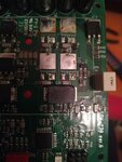
So i got electronic control box that controls 2 actuators for rising and lowering platform... The guy told me that one guy was inside and push the button for lowering while another one accidentaly pushed the button on the wireless remote for lifting the platform at the same time and control box stopped working... i was like, ok, probabbly short circuit on mosfets... i tested all the mosfets (IRLR3705), they are all ok, power supply ok, diodes also ok, transistors that controls mosfets also ok, but it just doesn't work... So i went down all to the mc-u, all the voltages are ok at the mcu... then another thing i dont understand... this H bridge, how does it works? i tracked down everything and i just don't get it how upper mosfets shift +12V from drain to source (drain on upper mosfets is constantly under 12V)? It has npn transistors for controlling upper mosfets and from my point of view that transistors connect ground to gates of upper mosfets but how this circuit turns ON thoose mosfets and shifts 12V to source? Sources of thoose 2 upper mosfets are going directly to actuator... I tried to trace if maybe it was multilayer board, but gates are not connected to anything except for thoose small NPN transistors... am i missing something obvious?
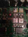
elec.jpg

elec2.jpg
 

for H bridge description:

https://www.modularcircuits.com/blog/articles/h-bridge-secrets/h-bridges-the-basics/

do you have a part number for the H Bridge you're talking about?

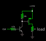
if the supply is 12V, then a resistor can pull the gate up and a transistor can pull it down
transistor ON, gate low, FET OFF
transistor OFF, gate pulled high by resistor, FET ON
it will likely be necessary to protect the gate on the upper FET from too low a voltage - a diode between the gate and ground should do.
the bridge circuit may have that built in gate protection diodes
 

From your description...
This could be the way NPN drives a high-side mosfet. A high-side P-device is not turned off unless the bias pin receives sufficiently high voltage (in other words, supply voltage).

P-device controlled by NPN.png

But on the other hand your number IRLR3705 is N type mosfet. A bootstrap circuit is often added in order to provide high enough voltage to turn on a high-side N device.
 

Well you can take a look at the picture, maybe i am missing something but i dont see bootstrap or charge pump anywhere... They all are n channel mosfets... I removed them for testing, but they are ok... I tested almoust everything on the board, nothing is faulty but it doesnt work. Maybe mc died, but i cant see a reason... I understand how h bridge works, but i cant see how this speciffic one works, to be more accurate how upper mosfets connects 12V from drain to source ... If you want i can take more photos
 

There's still your first idea about extreme current going through the mosfets. Did it blow a fuse? Did a copper trace break or open up?
Did a solder joint break? Etc.
 

To make NPN's control an H-bridge made entirely from N-devices, biasing can be done through various means:

* NPN carries bias directly to gate of Nmos. Turning on one turns on the other.
(At other times hold Nmos gate low by pulldown resistor.)

* (Nmos turned ON via gate held high by pullup resistor.) Arrange NPN to pull Nmos gate to ground. Then turn ON NPN to turn OFF Nmos.

One NPN can control a second Nmos in either column of the H-bridge.

A strategically-placed resistor can auto-bias a transistor.
 

that is clear to me, but i can't find pullup resistor anywhere... that's what is confusing me :(
 

pull up resistor:

one end is tied to the voltage you want pulled up to
in your case, its the voltage to drive the gate of the FET to turn it on.

the other end of the resistor is tied to the gate of the FET
AND, as gleaned from the discussion, the collector of an NPN transistor

the emitter is tied to ground (or the local low voltage that will turn OFF the FET)
in your case, the source of the FET

the base is tied to a control line, that, relative to the emitter will turn the NPN on or off.
when the NPN is ON, the FET will be OFF
when the NPN is OFF, the FET will be ON

http://en.wikipedia.org/wiki/Pull-up_resistor

http://www.learningaboutelectronics.com/Articles/How-to-connect-a-pull-up-resistor.php
 

Status
Not open for further replies.

Part and Inventory Search

Welcome to EDABoard.com

Sponsor

Back
Top