Welcome to our site! EDAboard.com is an international Electronics Discussion Forum focused on EDA software, circuits, schematics, books, theory, papers, asic, pld, 8051, DSP, Network, RF, Analog Design, PCB, Service Manuals... and a whole lot more! To participate you need to register. Registration is free. Click here to register now.
I have not used the mesh style specifically. To me it
looks too generalized. For the kind of products I do,
at least.
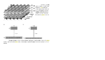
If you have a "from" and a "to" then you want to
connect at shortest loop / path length and as fat
as you can stand. Wide metal comes with slotting
rules that limits you to about 90% fill factor in the
bus itself. Fill factor in the cartoon looks like 50%.
But whether this matters depends on the circuit
and care-abouts. Me doing drivers and DC-DC
POL chips, for 125C and amps of time averaged DC
current, I care about ohmic drops and current
density for reliability, so I pave it wide and multiple
layers with built in decoupling by sandwiching.
Same as this mesh but higher conduction and
capacitance density.
But someone doing RF might care less about
ohms and more about femtofarads, and someone
working in fabs where pattern density is dictated
within small windows (not chip scale average)
might really like a "correct by construction" bus
tile cell that resembles the cartoon, modified
to suit -your- goals and constraints.
Take what you like from it but don't call it a
prescription.
This site uses cookies to help personalise content, tailor your experience and to keep you logged in if you register.
By continuing to use this site, you are consenting to our use of cookies.