Welcome to our site! EDAboard.com is an international Electronics Discussion Forum focused on EDA software, circuits, schematics, books, theory, papers, asic, pld, 8051, DSP, Network, RF, Analog Design, PCB, Service Manuals... and a whole lot more! To participate you need to register. Registration is free. Click here to register now.
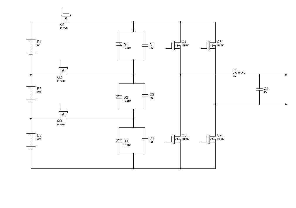
I'm having very hard time writing code for pic16f877a for my solar powered multilevel inverter with the above switching strategy. Can someone help me write this code? PLEASEEEE...:idea:
Your timing scheme has 14 steps. Create 7 arrays named SW1(), SW2(), etc.
In each array create 14 elements which contain the successive state (0 or 1) of that switch.
Go through a for-next loop X=1 to 14.
Examine SW1(X). If it's 1, then turn it on. If zero then turn it off.
A question....
* Do you want to write code on your own? --> then start with an idea, a piece of paper, a pencil, a flow chart....
* Or do you want someone else write code for you? --> then consider to pay for it.
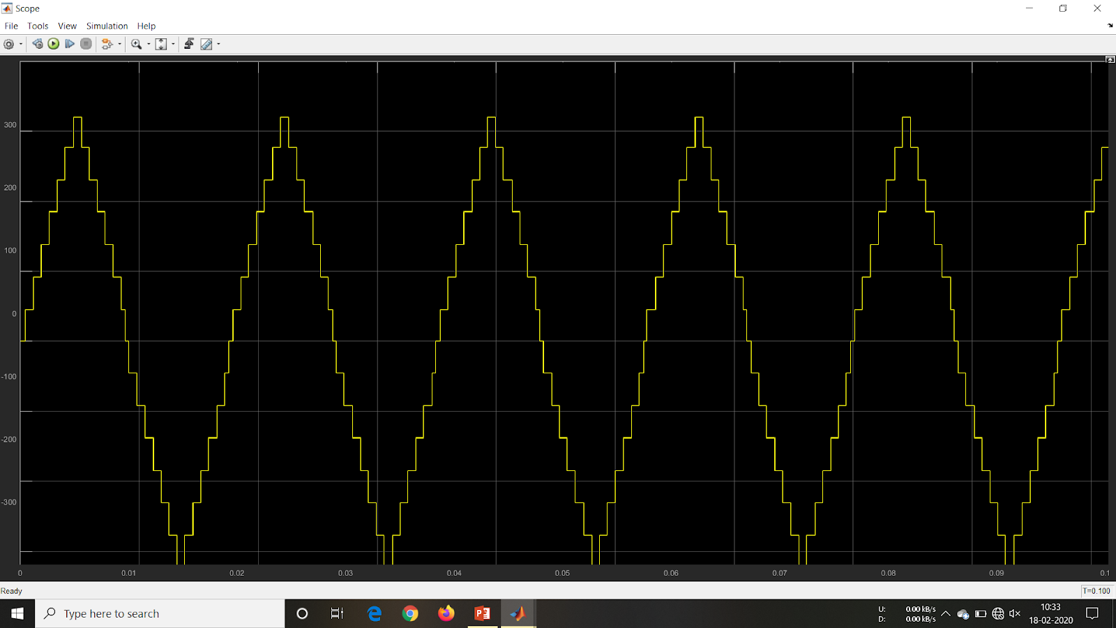
I have written this code for PIC16f877a but the output waveform is distorted. I'm a beginner in programming. Can you suggest what I am doing wrong so that I could get a correct output at 50Hz.
Code:
/*
* File: main.c
* Author: Group No 7 (SRMGPC)
* Created on 21 May, 2020, 1:39 PM
*/
#define _XTAL_FREQ 10000000
#pragma config FOSC = HS // Oscillator Selection bits (HS oscillator)
#pragma config WDTE = OFF // Watchdog Timer Enable bit (WDT disabled)
#pragma config PWRTE = OFF      // Power-up Timer Enable bit (PWRT disabled)
#pragma config BOREN = ON       // Brown-out Reset Enable bit (BOR enabled)
#pragma config LVP = OFF        // Low-Voltage (Single-Supply) In-Circuit Serial Programming Enable bit (RB3 is digital I/O, HV on MCLR must be used for programming)
#pragma config CPD = OFF        // Data EEPROM Memory Code Protection bit (Data EEPROM code protection off)
#pragma config WRT = OFF        // Flash Program Memory Write Enable bits (Write protection off; all program memory may be written to by EECON control)
#pragma config CP = OFF
#include <xc.h>
int level = 0;
int main() {
    TRISB = 0x00;               // set PORT B for output
    PORTB = 0b01001000;         // pin 7 and pin 4 of PORT B is high
    OPTION_REG = 0b00000111;    // set the prescalar to 256
    TMR0 = 244;                 // register value calculated for 0.01 ms delay
    TMR0IE = 1;
    GIE = 1;                    //enable global interrupt
    PEIE = 1;
    while(1) {
        if(level == 6) {
            RB3 = !RB3;     //switching T1
            RB6 = !RB6;     //switching T4
             RB4 = !RB4;     //switching T2
            RB5 = !RB5;     //switching T3
        }
        RB0 = !RB0;         //switching S1
        if(level % 2 != 0) {
            RB1 = !RB1;     //switching S2
        }
        if(level % 4 == 0) {
            RB2 = !RB2;     //switching S3
        }
        level++;
        if(level > 15) {
            level = 0;
        }
    }
    return 0;
}
void __interrupt() timer_isr(void) {
    if(TMR0IF == 1) {   // set timer value on overflow
        TMR0 = 244;     //timer value decrease to 0
        TMR0IF = 0;     //reset the timer interrupt
    }
}
This site uses cookies to help personalise content, tailor your experience and to keep you logged in if you register.
By continuing to use this site, you are consenting to our use of cookies.