Neelsama
Newbie level 3
Hello,
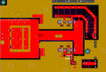
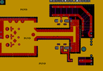
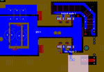
I am designing a new PCB for LLC converter and I just finishend laying out the H-Bridge for the input section. The PCB is 4 layer and primary side is rated for 500V/6A. Switching freq. is around 100kHz. I used TO 247-4 MOSFETs for H-Bridge. I named positive input to HV+ and negative input as PGND. Switch nodes are also shown below. Furthermore, I have tried to lay HV+ and switch nodes in parallel in both top and bottom side. Both of middle layers are PGND. I have etched the ground planes behind the switch nodes to reduce ground coupling.
Overall View:

Top layer:
Middle laye 2&3:
Bottom Layer:
I would appreciate your inputs how to further improve the layout in order to minimize stray inductance and decrease ground power coupling.
I am designing a new PCB for LLC converter and I just finishend laying out the H-Bridge for the input section. The PCB is 4 layer and primary side is rated for 500V/6A. Switching freq. is around 100kHz. I used TO 247-4 MOSFETs for H-Bridge. I named positive input to HV+ and negative input as PGND. Switch nodes are also shown below. Furthermore, I have tried to lay HV+ and switch nodes in parallel in both top and bottom side. Both of middle layers are PGND. I have etched the ground planes behind the switch nodes to reduce ground coupling.
Overall View:

Top layer:

Middle laye 2&3:

Bottom Layer:

I would appreciate your inputs how to further improve the layout in order to minimize stray inductance and decrease ground power coupling.