King_Ruzin
Newbie level 3
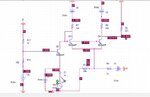
Hello everyone,
as a part of a course in analog circuits, I need to design a BJT amplifer with the following parameters:
Voltage gain = 51[dB]
Rin = 55[ohm]
Rout = 50[kohm]
Band width: [10kHz,1MHz]
DC suppliers allowed: +/- 5V
The purpose is to as less stages as possible.
I thought about using two stages : of CB and CE or 2 stages of CB.
the problem is when I tried to obtain bias point, I didnt manage to keep the circuit working propperly while maintaning the requested resistancies and gain.
I would appreciate any kind of help!
thanks guys.