Continue to Site

Welcome to EDAboard.com

Welcome to our site! EDAboard.com is an international Electronics Discussion Forum focused on EDA software, circuits, schematics, books, theory, papers, asic, pld, 8051, DSP, Network, RF, Analog Design, PCB, Service Manuals... and a whole lot more! To participate you need to register. Registration is free. Click here to register now.

Need to reduce drain voltage spike in LM5019 Buck converter

Status
Not open for further replies.
T

treez

Guest
Hi,
We are using the LM5019 for a Buck converter
Vin = 60V
Vout = 12V
Iout = 7mA

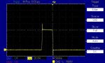
We notice a spike on the LM5019 drain voltage of 20V in magnitude...as in the attached. This surprises us, as the hi side FET is a N-channel mosfet. (so it should have a diode with cathode connected to vin.)

Can you see any reason why we cannot place a super fast rectifier from Drain to vin of LM5019, in order to staunch this spike?

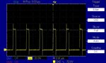
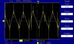
As you can also see, the inductor current is bi-directional (seen here in a 4R7 in series with the Buck inductor)

LM5019 monolithic synchronous buck converter datasheet:
https://www.ti.com/lit/ds/symlink/lm5019.pdf
 

Attachments

  • LM5019 drain _1.jpg
    LM5019 drain _1.jpg
    100.2 KB · Views: 106
  • LM5019 drain.jpg
    LM5019 drain.jpg
    107.6 KB · Views: 114
  • inductor current _4R7 sense.jpg
    inductor current _4R7 sense.jpg
    125.5 KB · Views: 104

could be partially your scope - see how you have a spike on the current - where no spike should be - e.g. at turn off the current simply cannot jump high - so there is some artifact on your scope - you need the short probe tip and a gnd spike right ( < 15mm ) on the o/p and gnd right at the chip to see a clean signal ...!

- but a small RC snubber should sort it 150pF 470 ohm ... for starters

- - - Updated - - -

also - try an external 100V "schottky" diode from gnd to the inductor - this will take some load off the chip and may help ...

- - - Updated - - -

Also Vin needs 4u7 MLCC X7R right at the pins ...
 
  • Like
Reactions: treez

    T

    Points: 2
    Helpful Answer Positive Rating
Thanks, it seems a little odd that in the datasheet "ABS MAX's" it says the SW pin should be no higher than "vin+0.3v".......whereas the vin pin can be up to 100v......so why cant the SW pin be exposed to 100V too? (even if the vin is only actually 60v).
I must admit it seems odd that the diode hasnt clamped the sw pin to vin, but as you say it coudl be a scope artefact.....this was scoped with a kynar twisted pair flying probe soldered to SW (and gnd) and the gnd wrapped around the scope ground barrel and the SW wrapped tightly to the probe tip...ie scope "gangling" gnd clip not used.

- - - Updated - - -

I have 1uF MLCC right on the Vin pin.
There is a further 5.4uF further away from the LM5019...though they are the othger side of a small 0805 ferrite bead
 

Hi

I don't think the peaks are real.
Rather a measurement artefact.
Show a photo of the circuit including scope connections.

Klaus
 
  • Like
Reactions: treez

    T

    Points: 2
    Helpful Answer Positive Rating
if you short your "probe" on the Vin line and still see the spikes - you know it is the probing system - you can subtract the artifact spikes from the signal.

you can also short your probe on the LHS of the choke and see if the artifact is there too ...
 
  • Like
Reactions: treez

    T

    Points: 2
    Helpful Answer Positive Rating
Status
Not open for further replies.

Similar threads

Part and Inventory Search

Welcome to EDABoard.com

Sponsor

Back
Top