firasgany7
Junior Member level 1
Hi guys,
I'm trying to design a transimpedance amplifier for optical receiver, based on this acrticle:
https://www.ti.com/lit/an/snoa515a/snoa515a.pdf
the requirements:
-VDDA=1.8V
-Cload = 200fF (the output of the amp loaded by 200fF)
-the total gain At=Vout/Ipd = 3000[Ohm], (Ipd is the current source on the left on the schematic)
-BW>20Mhz
this is the schematic AFTER I closed the loop:
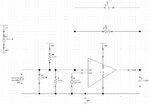
*there is also a reference current source ICP (100u) inside the OTA.
*the value of Rf is 3k[ohm]
*miller capacitor (in the OTA schematic) was put for stability purposes.
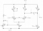
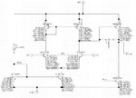
first I reached a good operation point where all transistors are in saturation. the open loop gain was (81 dB) with a BW 30kHz. (Open Loop without the feedback loading which means without the resistor Rf and the capacitor Cf, and without the input resistance r0,r1).
the I measured Open Loop with the feedback loading I get: 47dB Gain and BW of 230kHz.
Lastly, I closed the Loop I got the following: 73dB Gain and BW of 20kHz.
how do I achieve 20 Mhz bandwidth in Closed Loop? what are the changes that I need to do in the circuit to make that happen? I tried to play with W,L,gm of transistors at the output of the OTA.. I didn't recognize a certain pattern/effect.
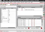
here are some details about the sizes of transistors and some parameters:


I'm trying to design a transimpedance amplifier for optical receiver, based on this acrticle:
https://www.ti.com/lit/an/snoa515a/snoa515a.pdf
the requirements:
-VDDA=1.8V
-Cload = 200fF (the output of the amp loaded by 200fF)
-the total gain At=Vout/Ipd = 3000[Ohm], (Ipd is the current source on the left on the schematic)
-BW>20Mhz
this is the schematic AFTER I closed the loop:

*there is also a reference current source ICP (100u) inside the OTA.
*the value of Rf is 3k[ohm]
*miller capacitor (in the OTA schematic) was put for stability purposes.
first I reached a good operation point where all transistors are in saturation. the open loop gain was (81 dB) with a BW 30kHz. (Open Loop without the feedback loading which means without the resistor Rf and the capacitor Cf, and without the input resistance r0,r1).
the I measured Open Loop with the feedback loading I get: 47dB Gain and BW of 230kHz.
Lastly, I closed the Loop I got the following: 73dB Gain and BW of 20kHz.
how do I achieve 20 Mhz bandwidth in Closed Loop? what are the changes that I need to do in the circuit to make that happen? I tried to play with W,L,gm of transistors at the output of the OTA.. I didn't recognize a certain pattern/effect.
here are some details about the sizes of transistors and some parameters:
