simon.vdw
Newbie level 1
Hi everyone,
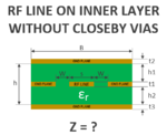
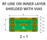
I have been searching for quite a while about the following subject, but can´t seem to find a decent answer on this. Imagine a 4-layer PCB (Top layer, Mid1 layer, Mid2 layer, Bottom layer). Mid1 layer and Bottom layer are GND panes with here and there vias to pass signals from the top layer to the Mid2 layer and back. RF signals on the top layer are done using CPWG. RF signals on the Mid2 layer are done with stripline or - and now comes the tricky part - striplines surrounded by GND planes as well. My question louds: What is the characteristic impedance of these kind of RF lines? Note that these kind of RF lines are no ordinary striplines, but rather striplines + surrounded by GND Planes at both sides, so similar to a CPWG, with GND plane also above the RF line. I have add two images to clarify.
Thanks and best regards
Simon

