Junus2012
Advanced Member level 5
Dear friends,
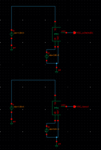
I am trying to design a MOS pseudo resistor to use it as an average resistor for the CMFB ampliifer rather than using the big poly resistor, I am using the one shown in the schematc becture below.

for the test I am simulating I am simulating by a DC source a differential voltage to the resistor terminal, Note that GND pin is only needed for the layout purpose to connect the P-Wafer to the ground and has nothing to do with the circuit. The simulation setup and schematic result are shown below. As you see from the result, the resistor is quite good and linear for the entire differential region.


Afterthen I did the layout with no LVS error as shown below

Now the post layout simulation is something very diviated from the schematic one as shown below

I wouls expect a change from layout but not as huge as this one,
I would appreciate your help in this manner
thanks
I am trying to design a MOS pseudo resistor to use it as an average resistor for the CMFB ampliifer rather than using the big poly resistor, I am using the one shown in the schematc becture below.

for the test I am simulating I am simulating by a DC source a differential voltage to the resistor terminal, Note that GND pin is only needed for the layout purpose to connect the P-Wafer to the ground and has nothing to do with the circuit. The simulation setup and schematic result are shown below. As you see from the result, the resistor is quite good and linear for the entire differential region.

Afterthen I did the layout with no LVS error as shown below

Now the post layout simulation is something very diviated from the schematic one as shown below
I wouls expect a change from layout but not as huge as this one,
I would appreciate your help in this manner
thanks