arr_baobao
Full Member level 2
Hi guy,
i'm currently doing pcb simulation with CST. i have some basic question to ask here.
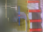
let say i assign a discrete port in my PCB for a series component as shown in figure below

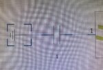
In schematic tab i assign this discrete port as lump component. the connection is shown in below. am i doing it right, by terminating the other end with a ground.
one more question if i replace it with a series resistor, i wanna probe the signal after the series resistor, which side i should place the probe in schematic tab, the ground site or the other side?

hope someone here can answer my question.
thanks
i'm currently doing pcb simulation with CST. i have some basic question to ask here.
let say i assign a discrete port in my PCB for a series component as shown in figure below

In schematic tab i assign this discrete port as lump component. the connection is shown in below. am i doing it right, by terminating the other end with a ground.
one more question if i replace it with a series resistor, i wanna probe the signal after the series resistor, which side i should place the probe in schematic tab, the ground site or the other side?

hope someone here can answer my question.
thanks