Continue to Site

Welcome to EDAboard.com

Welcome to our site! EDAboard.com is an international Electronics Discussion Forum focused on EDA software, circuits, schematics, books, theory, papers, asic, pld, 8051, DSP, Network, RF, Analog Design, PCB, Service Manuals... and a whole lot more! To participate you need to register. Registration is free. Click here to register now.

Charge Pump with unity gain amplifier (Bootstrapping Charge Pump)

Status
Not open for further replies.

firasgany7

Junior Member level 1
Joined
Oct 11, 2019
Messages
19
Helped
0
Reputation
0
Reaction score
0
Trophy points
1
Activity points
209
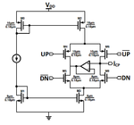
Im trying to understand the the benefits of Charge Pump with unity gain amplifier compared to the normal charge pump that is implemented using two current mirrors:
11.png

we have few questions about this circuit:

1) how does the unity gain amplifier helps me get higher input impedance in order to have more constant current? (this is called bootstrapping circuit)
2) how does keeping the same VDS for M4 and M6 the same through the amplifier with feedback helps solve the current mismatch problem?
3) Why is this circuit is more suitable to work with Low Swing inputs?

I attached some references that deal with this design if they can help you get better picture.
 

Attachments

  • DESIGN OF A PHASE FREQUENCY DETECTOR AND CHARGE PUMP FOR A PHASE-LOCKED LOOP IN 0.18µm CMOS (...pdf
    4.3 MB · Views: 290
  • Analysis and Design of Charge Pumps for Tellecommunication Apps (with amplifier).pdf
    378.4 KB · Views: 229
  • DESIGN OF A PHASE LOCKED LOOP BASED CLOCKING CIRCUIT FOR HIGH SPEED SERIAL LINK APPLICATIONS (wi.pdf
    5.1 MB · Views: 265

The opamp doesn't really help with having higher impedance of the current sources. The impedance is what it is coming from the gds of the transistors M2/M3. What it helps with is keeping the current source transistors under same conditions no matter which switch is on or off. If there was no buffer and respectively if you didn't have the left branch of switches, then when M6 is off and M8 on, the PMOS current source M2 will have Vds=0v. Next time M6 turns on, you will have to charge the drain of M2 and that charge will come from the charge pump output capacitor, which means ripple on the control voltage of the VCO, which means spurs in the output frequency.
With the buffer and the left branch of switches, when M6 is off, M4 is on and the current of M2 continues flowing keeping the M2 drain voltage unchanged.
 

Hi,
thanks for your reply.
can you please explain why:
when M6 is off and M8 on, the PMOS current source M2 will have Vds=0v.
?
assuming that the current mirror M0/M2 is in saturation then there is no situation where no current necissarily mean VDS=0.
 

Well, you have M0 driving the gate of M2, but the path for the drain current is cut off by turning off M6 (assuming no opamp and no M4/5). That can only result of M2 Vds=0.
 

so, if I understand you right, you are saying the current mirror forces (Vgs-Vt) to be the same on M0 and M2 and it cant be zero, and the only way to make no current is when M2 is in linear and VDS=0?
 

Yes, that's right. There are two conditions for a MOS transistor to be in saturation:
1) to have some Vgs-Vth
2) to have enough Vds.
Here, when M6 is off, the second condition is not valid. It is the same as when you connect very big resistance to the drain of a transistor. Pictorially, it moves the transistor to the origin of its Id-Vds curve (for the given Vgs) and there it is in triode with 0 current.
 

Hi there,
After going through what you wrote I'm trying to justify when the following statement is right:
Next time M6 turns on, you will have to charge the drain of M2 and that charge will come from the charge pump output capacitor
why this would happen?
the way I think of it is a a situation where M8 is OFF, and M6 changes from OFF to ON, that way would be charge sharing between Vcp,Out and the M2 drain node. (we assume there is a capacitor C,m2 there).
the previous state is the state when Down=0, and Up=1, its the situation where M6 is ON and M8 is OFF, and the charge pump should be charging, according to your explanation some that charge gets wasted to Charge Sharing if the analysis I did was right.
Thanks,
Firas
 

Yes, there is charge sharing and that's the problem.
Imagine a hypothetical situation where we have the charge pump with its output capacitor and the VCO only. Let's say the charge pump output cap is charged to some voltage and the Cm2 is charged to supply with M6 off (we don't care now about M2). When M6 turns on the charge pump output voltage will step up, increasing the VCO frequency.
When the PLL loop is closed we want to have controlled charge or discharge of the charge pump capacitor with a fixed current. However, because we have charge sharing the output voltage steps up a bit and then the current of M2 continues charging it. If the loop doesn't correct it, the VCO frequency will be not what we wanted. But since we have an infinite gain integrator in the loop (i.e. the charge pump) it will have to make the average voltage controlling the VCO such that the average frequency out of the VCO is equal to the ref frequency. To compensate for the charge injection the loop will create a phase offset between the input and VCO frequency in the locked state. This is done by making the UP pulses wider/shorter compared to the DN pulses. However this will result in ripple of the VCO control voltage and respectively spurs in the output frequency spectrum.

From a different perspective - PLL loop is very much like opamp loop, say with unity feedback. Imagine a 2 stage opamp, the first stage is an OTA, loaded with a big cap to ground and then there is the second stage (we don't care here if it is Miller compensated or just the cap to gnd between the two stages is large enough to provide for stability). Now imagine that there is a small current besides the current coming from the 1st stage OTA that also gets dumped into the capacitor. When we close the feedback loop, it will want to make the two inputs of the 1st stage equal i.e. virtual short. But if it does, then the extra current into the capacitor will drift the output of the 1st stage away from the point of virtual short. So, the loop works such that it creates an offset at the input of the opamp that tilts the input diff pair so that it compensates for the extra current and the capacitor is charged to a voltage that provides for the equilibrium in the system.
 

Status
Not open for further replies.

Similar threads

Part and Inventory Search

Welcome to EDABoard.com

Sponsor

Back
Top