Continue to Site

Welcome to EDAboard.com

Welcome to our site! EDAboard.com is an international Electronics Discussion Forum focused on EDA software, circuits, schematics, books, theory, papers, asic, pld, 8051, DSP, Network, RF, Analog Design, PCB, Service Manuals... and a whole lot more! To participate you need to register. Registration is free. Click here to register now.

Fully-Differential folded cascode amplifier with enhanced gain

Status
Not open for further replies.

Junus2012

Advanced Member level 5
Joined
Jan 9, 2012
Messages
1,552
Helped
47
Reputation
98
Reaction score
53
Trophy points
1,328
Location
Italy
Activity points
15,235
Hello,

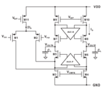
I am interesting on enhancing the gain of the fully differential folded cascode amplifier as shown in the figure below,

For the auxilary boost amplifier (AUX-N and AUX-B) I would like to use folded cascode amplifier. As these auxilary amplifiers are also fully differential amplifier they requires a CMFB as well.

For the main amplifier it is very obvoius to use a CMFB amplifier that compare with VCM, which is typically VDD/2 for my application.

My question is :

What is the value of the common mode voltage to compare for the AUX differential amplifier CMFB ?

Thank you
enhanced gain.PNG
 

Imagine that M5-M8 are simple cascode transistors, and the AUX-N/AUX-P set now the cascode bias voltages, which should be a Vgs+Vdsat for a folded-cascode amp with not enhanced gain to reach the highest output swing. Thus they should get a Vgs+Vdsat as Vcm, I think.
 
Imagine that M5-M8 are simple cascode transistors, and the AUX-N/AUX-P set now the cascode bias voltages, which should be a Vgs+Vdsat for a folded-cascode amp with not enhanced gain to reach the highest output swing. Thus they should get a Vgs+Vdsat as Vcm, I think.

Dear frank,

I confirmed from your answer that we can not use the output VCM as a reference voltage for the boosting auxilary ampliifer, and I believe that your relationship is mostly correct, only I am suspecting the use Vdsat in your given formula, because at the steady state operation we will get an actual VDS while VDS sat represent the minimum VDS for saturation region.

What about mesuring it by simulation, from DC analyses I measure the DC voltage at the gate of M5-M6, so that VCM(Auxilary-P)= VG5,6
similarly VCM(Auxilary-N)=VDD-VG7,8

Am I right ?

What about using un referenced fully differential amplifier for the auxilary ampliifer (the type of fully differential amplifier which can set the VOC level without using CMFB)

Thank you
 

You should not try to somehow fudge the common-mode voltage of the aux amplifier. Best is to create a replica circuit from similar transistors as M3 and M5, with a current that's also similar (DC value) as the one in the main amp. Then use this replica to create the reference voltage to set the common-mode of the aux amplifier.
 
You should not try to somehow fudge the common-mode voltage of the aux amplifier. Best is to create a replica circuit from similar transistors as M3 and M5, with a current that's also similar (DC value) as the one in the main amp. Then use this replica to create the reference voltage to set the common-mode of the aux amplifier.

Dear Suta,

T'hank you for your reply and nice to see you again,

I appreciate your help but indeed I didn't get your point, can you please explain it again in different way
 

You need to create a voltage reference for your CMFB circuit for the aux amps that puts the main amplifier cascodes in the right operating conditions. An idea could be with a replica circuit like in the picture, which is just an example. The goal is to track the cascodes voltage in process and temperature. The gate of M3a should connect to the same voltage as the gate of M3, of course.

**broken link removed**

Thank you Suta for your reply,

Yes for sure I have to connect the CMFB of each auxilary ampliifer to a reference voltage, I will call it VCM_N for AUX-N and VCM_P for AUX-P, and this is the origional of my question, how to define these voltages ?
Also you referred in your answer to circuit that have M3a which is not shown
Thank you
 

I see this time it worked. So, just a clarification. The replica is there to just make sure the operating conditions for M5a and M3a are good with the cascode bias of M5a. Then, for the common-mode reference voltage you can only use the long chain of diode transistor biasing the gate of M5a.
 
I see this time it worked. So, just a clarification. The replica is there to just make sure the operating conditions for M5a and M3a are good with the cascode bias of M5a. Then, for the common-mode reference voltage you can only use the long chain of diode transistor biasing the gate of M5a.

Dear Suta,

Thank you for your reply

I understnd from your explanation and graph that I need to set VCM_N for AUX-N to the same gate level of M5, which is the biasing voltage of the NMOS cascoded mirror, the same for the upper AUX-P,

Basically and ideally this voltage is equal to 2VDS(sat)+Vth for the NMOS mirror and VDD-[2VSD(sat)+Vth] for the PMOS mirror, right ?
 

Yes. Try it and let me know what you get.

Thank you Suta,

I would like to confirm your aswer because also I have read now similar thing in Jakob book,

My next question please,

The common mode feedback amplifier for both AUX-P and AUX-N must have an input common mode range that accept the reference voltage (VCM_N & VCM_P). For this reason, the common-mode amplifier that compare the VCM_N= 2VDS(sat)+Vth for the NMOS mirror should be PMOS input stage. Using this principle, the common mode amplifier for the PMOS cascode mirror should have NMOS input stage. For the latter one even both NMOS or PMOS input stage can work

Please correct me if I am wrong
Thank you again
 

It sounds about right. If you are still working with 0.35um technology, the gate of the NMOS cascodes will be at something like 2*0.2+0.6=1V and for a supply of 3.3V that will be better handled by a PMOS input diff stage for the Aux amplifier.
 
Exactly right. That's why in my previous comment I said that "The replica is there to just make sure the operating conditions for M5a and M3a are good with the cascode bias of M5a." Or if you want to be more fancy, you can come up with a circuit that automatically adjusts the gate voltage of the replica such, that M3a has good Vds. Then slave that gate voltage as a reference for the CMFB amp. But that's unnecessary complication.
 
Status
Not open for further replies.

Part and Inventory Search

Welcome to EDABoard.com

Sponsor

Back
Top