eduardoAvelar
Newbie level 6
- Joined
- Dec 11, 2017
- Messages
- 11
- Helped
- 0
- Reputation
- 0
- Reaction score
- 0
- Trophy points
- 1
- Location
- MG, Brazil
- Activity points
- 154
Hi all!
I'm trying to design an inverter in Half-Bridge topology and it should have sinusoidal wave output with 30Vdc In and 15Vdc máx output.

I have tried two different types of modulation.
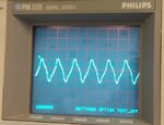
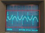
The first one uses a complementary sPWM with dead time about 300ns between pulses. This should be seen in the first and second pictures below. The real results of this kind of modulation it's exposed on the third picture.


The other type of modulation uses a single modulation method when each MOSFET can receive the pulses individually half of the period.
The results are indicated in the subsequent pictures.


Both tests are made with approximately 23Khz of modulation.
The output LC filter was calculated and the values are 1.6mH and 45uF. I'm testing with 1.2mH and 30uF.
I have a doubt about the output using the complementary type of modulation.

Does you guys have some idea, based on data exposed, about why the output waveform is having that shape?
Thanks in advance
I'm trying to design an inverter in Half-Bridge topology and it should have sinusoidal wave output with 30Vdc In and 15Vdc máx output.

I have tried two different types of modulation.
The first one uses a complementary sPWM with dead time about 300ns between pulses. This should be seen in the first and second pictures below. The real results of this kind of modulation it's exposed on the third picture.
Code:
volatile static char theTCCR1A = 0b10110010; //varible for TCCR1A
volatile char cycle = 1;

// 200 pontos, valor de pico de 240, offset 0
int lookUp_1[] = {5, 9, 13, 16, 20, 24, 28, 31, 35, 39, 43, 46, 50, 54, 57, 61, 65, 68, 72, 76, 79, 83, 86, 90, 93, 97, 100, 104, 107, 111, 114, 117, 121, 124, 127, 130, 134, 137, 140, 143, 146, 149, 152, 155, 158, 161, 164, 167, 169, 172, 175, 177, 180, 183, 185, 187, 190, 192, 195, 197, 199, 201, 203, 206, 208, 210, 212, 213, 215, 217, 219, 221, 222, 224, 225, 227, 228, 230, 231, 232, 233, 234, 235, 236, 237, 238, 239, 240, 241, 241, 242, 243, 243, 244, 244, 244, 245, 245, 245, 245, 245, 245, 245, 245, 245, 244, 244, 244, 243, 243, 242, 241, 241, 240, 239, 238, 237, 236, 235, 234, 233, 232, 231, 230, 228, 227, 225, 224, 222, 221, 219, 217, 215, 213, 212, 210, 208, 206, 203, 201, 199, 197, 195, 192, 190, 187, 185, 183, 180, 177, 175, 172, 169, 167, 164, 161, 158, 155, 152, 149, 146, 143, 140, 137, 134, 130, 127, 124, 121, 117, 114, 111, 107, 104, 100, 97, 93, 90, 86, 83, 79, 76, 72, 68, 65, 61, 57, 54, 50, 46, 43, 39, 35, 31, 28, 24, 20, 16, 13, 9};
// 200 pontos, valor de pico de 240, offset 0
int lookUp_2[] = {0, 4, 8, 11, 15, 19, 23, 26, 30, 34, 38, 41, 45, 49, 52, 56, 60, 63, 67, 71, 74, 78, 81, 85, 88, 92, 95, 99, 102, 106, 109, 112, 116, 119, 122, 125, 129, 132, 135, 138, 141, 144, 147, 150, 153, 156, 159, 162, 164, 167, 170, 172, 175, 178, 180, 182, 185, 187, 190, 192, 194, 196, 198, 201, 203, 205, 207, 208, 210, 212, 214, 216, 217, 219, 220, 222, 223, 225, 226, 227, 228, 229, 230, 231, 232, 233, 234, 235, 236, 236, 237, 238, 238, 239, 239, 239, 240, 240, 240, 240, 240, 240, 240, 240, 240, 239, 239, 239, 238, 238, 237, 236, 236, 235, 234, 233, 232, 231, 230, 229, 228, 227, 226, 225, 223, 222, 220, 219, 217, 216, 214, 212, 210, 208, 207, 205, 203, 201, 198, 196, 194, 192, 190, 187, 185, 182, 180, 178, 175, 172, 170, 167, 164, 162, 159, 156, 153, 150, 147, 144, 141, 138, 135, 132, 129, 125, 122, 119, 116, 112, 109, 106, 102, 99, 95, 92, 88, 85, 81, 78, 74, 71, 67, 63, 60, 56, 52, 49, 45, 41, 38, 34, 30, 26, 23, 19, 15, 11, 8, 4};

void setup() {

  TCCR1A = theTCCR1A; // 0b10110010;
  /*10 Desliga OC1A (D9) no valor de comparação, Liga OC1A em 0V (Modo Não Invertido) Tabela 15-3 Datasheet
    11 Liga OC1B (D10) no valor de comparação, Desliga OC1B em 0V (Modo Invertido)  Tabela 15-3 Datasheet
    00 Bits 3 e 2 Não possuem função
    10 WGM11=1 e WGM10=0 for waveform 10 - Phase Correct mode - Garante o tempo morto
  */
  // Timer Counter Control Register 1 A
  TCCR1B = 0b00010001;
  /*000
    10 WGM13=1 e WGM12=0 Para a forma de onda 10 Phase Corretc PWM mode
    001 Sem preescale para o contador.
  */
  // Timer Interrupt Mask Register 1
  TIMSK1 = 0b00000001;
  /*0000000
    1 TOV1 Flag interrupt enable.
  */
  ICR1 = 333;
  sei();             // Enable global interrupts.

  // Set outputs pins.
  // Data Direction Register PORTB
  // 1 -> Saída
  // 0 -> Entrada
  // Configura os pinos PB1(D9), PB2 (D10), PB3 (D11), PB4 (D12) como saidas
  DDRB   = 0b00011110;
  // Inicialização das saídas
  PORTB |= 0b00001000;
  PORTB &= 0b11101111;
}

void loop() {
}

// Interrupt Service Routine
ISR(TIMER1_OVF_vect) {
  static int num;
  static int i;
  static int delay1;
  static char trig;

  if (num >= 200) {
    TCCR1A ^= 0b01010000;

    if (cycle) {
      PORTB ^= 0b00001000;
      PORTB ^= 0b00010000;
    } else {
      PORTB ^= 0b00010000;
      PORTB ^= 0b00001000;
    }
    cycle  ^= 0b00000001;
    num = 0;
  }

  if (cycle) {
    OCR1A = lookUp_2[num];
    OCR1B = lookUp_1[num];
    num ++;
  } else {
    OCR1A = lookUp_1[num];
    OCR1B = lookUp_2[num];
    num ++;
  }
}


The other type of modulation uses a single modulation method when each MOSFET can receive the pulses individually half of the period.
The results are indicated in the subsequent pictures.
Code:
#define SinDivisions (350)// Sub divisions of sisusoidal wave.

static int microMHz = 16; // Micro clock frequency
static int freq = 60;     // Sinusoidal frequency
static long int period;   // Period of PWM in clock cycles.
static unsigned int lookUp[SinDivisions];
static char theTCCR1A = 0b10000010; //varible for TCCR1A

void setup() {
  double temp;

  period = microMHz * 1e6 / freq / SinDivisions; // Period of PWM in clock cycles

  for (int i = 0; i < SinDivisions / 2; i++) { // Generating the look up table.
    temp = sin(i * 2 * M_PI / SinDivisions) * period;
    lookUp[i] = (int)(temp + 0.5);     // Round to integer.
  }
  // Register initilisation, see datasheet for more detail.
  TCCR1A = theTCCR1A; // 0b10000010;
  TCCR1B = 0b00011001;
  TIMSK1 = 0b00000001;
  ICR1   = period;
  sei();             // Enable global interrupts.
  // Set outputs pins.
  // Set outputs pins.
  // Data Direction Register PORTB
  // 1 -> Saída
  // 0 -> Entrada
  // Configura os pinos PB1(D9), PB2 (D10), PB3 (D11), PB4 (D12) como saidas
  DDRB   = 0b00011110;
}

void loop() {
}

ISR(TIMER1_OVF_vect) {
  static int num;
  static int delay1;
  static char trig;

  if (delay1 == 1) {
    theTCCR1A ^= 0b10100000;
    TCCR1A = theTCCR1A;
    delay1 = 0;
  } else if (num >= SinDivisions / 2) {
    num = 0;
    delay1++;
    trig ^= 0b00000001;
    PORTB ^= 0b00010000;
  }
  OCR1A = OCR1B = lookUp[num];
  num++;
}

Both tests are made with approximately 23Khz of modulation.
The output LC filter was calculated and the values are 1.6mH and 45uF. I'm testing with 1.2mH and 30uF.
I have a doubt about the output using the complementary type of modulation.

Does you guys have some idea, based on data exposed, about why the output waveform is having that shape?
Thanks in advance