T
treez
Guest
Hi,
Our contractor has done a prototype 60W offline single stage, PFC’d Flyback (240VAC).
The primary FET is a metal tabbed TO220 and is directly screwed to an aluminium heatsink (no insulating pad used) . The heatsink is soldered into the PCB via two pins. The heatsink is obviously at drain node potential.
We sent the PCB for testing where it was put in a chamber at 70degC and run at max power and 190VAC input. After some time, the unit failed.
The unit was returned to me and I inspected it, to see what had gone wrong. The 3.15A input fuse had not blown, but a 3W, 2R7 inrush resistor just downstream of the fuse had blown open. There was a strange tarnishing on the PCB beneath the primary FET…however, the FET itself looked spotless. This tarnishing did not seem to be associated with any component, but was disappearing under the heatsink. Also, the primary FET G,D,S did not measure short to each other.
Anyway, I then replaced the 2R7 inrush resistor, and then powered the unit up , starting gingerly at zero VAC , and slowly raising it……at around 60VAC input, there was a fizzling sound, and so I immediately turned off the power source. I then found that the primary FET was short circuit between its pins.
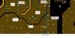
Therefore, I replaced the FET…and decided to see what the tarnishing was that was going under the heatsink. As can be seen in the attached picture of the PCB layer 2, the PCB was burned almost right through at the heatsink pin. (it’s a 4 layer 1.6mm thick PCB). Anyway, the burn crater had black burned carbonisation in it. Therefore, I scraped out the black carbonisation from the burn crater, and then blew away the carbon dust, to clean the crater. ..
Then, with the new PRIMARY FET in, I again powered the unit up on the AC source. This time it worked fine…no problem at 240VAC.
When at 190VAC and max power, the FET drain node goes up to 580Vpk. As you can see, the primary ground is only 0.25mm away from the plated through hole that contains the heatsink pin where the burn crater is. However, there are 3 other PTH’s where this also applys, and they didn’t suffer burning.
So anyway, do you suppose that the burning may be anything to do with flashover of the primary ground to the drain node copper at the heatsink pin? We are all agreed that 0.25mm is not enough clearance for 580Vpk on an internal PCB layer. However, there was no flashover at the other pins with similar clearances.
At our own premises, we have run this unit in the chamber on many occasions for 8 hours at 190VAC input, internal ambient of 70degc in the PSU enclosure, and max power and did not get any of this PCB burning, or any unit failure. We recorded FET case temp of 100degC.
Our contractor has done a prototype 60W offline single stage, PFC’d Flyback (240VAC).
The primary FET is a metal tabbed TO220 and is directly screwed to an aluminium heatsink (no insulating pad used) . The heatsink is soldered into the PCB via two pins. The heatsink is obviously at drain node potential.
We sent the PCB for testing where it was put in a chamber at 70degC and run at max power and 190VAC input. After some time, the unit failed.
The unit was returned to me and I inspected it, to see what had gone wrong. The 3.15A input fuse had not blown, but a 3W, 2R7 inrush resistor just downstream of the fuse had blown open. There was a strange tarnishing on the PCB beneath the primary FET…however, the FET itself looked spotless. This tarnishing did not seem to be associated with any component, but was disappearing under the heatsink. Also, the primary FET G,D,S did not measure short to each other.
Anyway, I then replaced the 2R7 inrush resistor, and then powered the unit up , starting gingerly at zero VAC , and slowly raising it……at around 60VAC input, there was a fizzling sound, and so I immediately turned off the power source. I then found that the primary FET was short circuit between its pins.
Therefore, I replaced the FET…and decided to see what the tarnishing was that was going under the heatsink. As can be seen in the attached picture of the PCB layer 2, the PCB was burned almost right through at the heatsink pin. (it’s a 4 layer 1.6mm thick PCB). Anyway, the burn crater had black burned carbonisation in it. Therefore, I scraped out the black carbonisation from the burn crater, and then blew away the carbon dust, to clean the crater. ..
Then, with the new PRIMARY FET in, I again powered the unit up on the AC source. This time it worked fine…no problem at 240VAC.
When at 190VAC and max power, the FET drain node goes up to 580Vpk. As you can see, the primary ground is only 0.25mm away from the plated through hole that contains the heatsink pin where the burn crater is. However, there are 3 other PTH’s where this also applys, and they didn’t suffer burning.
So anyway, do you suppose that the burning may be anything to do with flashover of the primary ground to the drain node copper at the heatsink pin? We are all agreed that 0.25mm is not enough clearance for 580Vpk on an internal PCB layer. However, there was no flashover at the other pins with similar clearances.
At our own premises, we have run this unit in the chamber on many occasions for 8 hours at 190VAC input, internal ambient of 70degc in the PSU enclosure, and max power and did not get any of this PCB burning, or any unit failure. We recorded FET case temp of 100degC.