seweihe
Newbie level 3
Hi everyone.
Background:
I'm a final year Mechanical and Mechatronic Engineering Student at the University of Cape Town and was tasked with designing a buck converter for a hexapod robot project amongst other things. Decided to use the LT3741 IC (https://www.analog.com/media/en/technical-documentation/data-sheets/37411fg.pdf) since it met the requirements of the system.
The buck convert should take 25V to 17V as an input from the battery and output 15V to the servos of the hexapod. The motors draw up to 8A maximum from prior testing and hence proceeded to add a bit of a safety margin and design with peak current draws of 10A. I then followed the design instructions of the datasheet pretty closely and created a document based on these instructions. Then proceeded to simulate the circuit in LTSpice and got it to operate as desired. After getting this working I drew up the schematic for the pcb along with a 5V buck converter and designed the PCB. Documentation regarding the design can be found attached including the calculations based on the datasheet as well as the schematic and PCB layout. I had the PCB layout looked over by a technical advisor in the department and he did not recognize any flaws based on his experience designing PCB's. I hence had the PCB's manufactured and components sourced and assembled the PCB.
Problem:
The buck converter using the LT3741 is not functioning correctly under load. Under no load the output is 15V and the waveforms at points in the circuit are as expected. When I apply a load the output voltage drops significantly and the switching breaks down periodically. When removing the load the buck converter remains in this unstable state. I have found a means of getting it back to normal operation by bridging my finger across the switching node and the RT pin(has a programming resistor connected to it for the oscillator that controls the switching frequency of the device) of the LT3741. Applying my finger across these points under load helps up to a point but once the current draw becomes higher the chip operates in the unstable state again. Looking at the RT pin on the oscilloscope quite large voltage spikes appear once in the unstable state as shown in these images.


Some examples of the unstable waveforms at the switching node are:


The output to the gates of the MOSFETs have similar waveforms:

Fixes I've tried:
-Adding a polymer cap to VCC_int capacitor (CVCC) to reduce capacitor ESR. The datasheet mentions this is important to reduce internal noise within the LT3741.
-Increasing Cin capacitor.
Possible Issues I've identified:
-the inductor is perhaps incorrectly sized at 4.7uH and perhaps a 3.3uH inductor would be more suitable.
-my PCB layout is absolutely terrible and there is too much noise being produced with the layout of the inductor and main traces close to the LT3741 and RT pin.
I would appreciate any advice and suggestions to fix this as well as any in-depth opinions on what the failure is with the design. Unfortunately, I've taught myself how to design PCB's for my final year project and luckily the other 3 I've designed have worked out but after a week of trying to problem solve the issue, I'm finding myself in need of some expert electrical engineering advice. Apologies for the long post, I was trying to provide as much information as possible with regard to the issue. Thanks in advance to anyone who's willing to help.
Background:
I'm a final year Mechanical and Mechatronic Engineering Student at the University of Cape Town and was tasked with designing a buck converter for a hexapod robot project amongst other things. Decided to use the LT3741 IC (https://www.analog.com/media/en/technical-documentation/data-sheets/37411fg.pdf) since it met the requirements of the system.
The buck convert should take 25V to 17V as an input from the battery and output 15V to the servos of the hexapod. The motors draw up to 8A maximum from prior testing and hence proceeded to add a bit of a safety margin and design with peak current draws of 10A. I then followed the design instructions of the datasheet pretty closely and created a document based on these instructions. Then proceeded to simulate the circuit in LTSpice and got it to operate as desired. After getting this working I drew up the schematic for the pcb along with a 5V buck converter and designed the PCB. Documentation regarding the design can be found attached including the calculations based on the datasheet as well as the schematic and PCB layout. I had the PCB layout looked over by a technical advisor in the department and he did not recognize any flaws based on his experience designing PCB's. I hence had the PCB's manufactured and components sourced and assembled the PCB.
Problem:
The buck converter using the LT3741 is not functioning correctly under load. Under no load the output is 15V and the waveforms at points in the circuit are as expected. When I apply a load the output voltage drops significantly and the switching breaks down periodically. When removing the load the buck converter remains in this unstable state. I have found a means of getting it back to normal operation by bridging my finger across the switching node and the RT pin(has a programming resistor connected to it for the oscillator that controls the switching frequency of the device) of the LT3741. Applying my finger across these points under load helps up to a point but once the current draw becomes higher the chip operates in the unstable state again. Looking at the RT pin on the oscilloscope quite large voltage spikes appear once in the unstable state as shown in these images.
Some examples of the unstable waveforms at the switching node are:
The output to the gates of the MOSFETs have similar waveforms:
Fixes I've tried:
-Adding a polymer cap to VCC_int capacitor (CVCC) to reduce capacitor ESR. The datasheet mentions this is important to reduce internal noise within the LT3741.
-Increasing Cin capacitor.
Possible Issues I've identified:
-the inductor is perhaps incorrectly sized at 4.7uH and perhaps a 3.3uH inductor would be more suitable.
-my PCB layout is absolutely terrible and there is too much noise being produced with the layout of the inductor and main traces close to the LT3741 and RT pin.
I would appreciate any advice and suggestions to fix this as well as any in-depth opinions on what the failure is with the design. Unfortunately, I've taught myself how to design PCB's for my final year project and luckily the other 3 I've designed have worked out but after a week of trying to problem solve the issue, I'm finding myself in need of some expert electrical engineering advice. Apologies for the long post, I was trying to provide as much information as possible with regard to the issue. Thanks in advance to anyone who's willing to help.
Attachments
-
DC-DC Buck Converter Calculations 20-09-2019.pdf896.9 KB · Views: 130
-
Hexapod DC-DC converter schematic.pdf115.2 KB · Views: 113
-
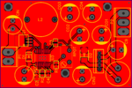 Hexapod PCB_DC-DC-Converter_Top.png449.6 KB · Views: 273
 -
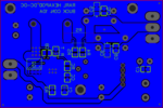 Hexapod PCB_DC-DC-Converter_Bottom.png380.9 KB · Views: 199
 -
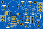 Hexapod DC-DC Top View Graphical.png492.9 KB · Views: 179
 -
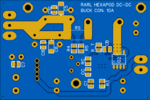 Hexapod DC-DC Bottom View Graphical.png408.6 KB · Views: 179
 -
 IMG_20190910_120030.jpg409 KB · Views: 193
 -
 IMG_20190913_164013.jpg452 KB · Views: 202