Continue to Site

Welcome to EDAboard.com

Welcome to our site! EDAboard.com is an international Electronics Discussion Forum focused on EDA software, circuits, schematics, books, theory, papers, asic, pld, 8051, DSP, Network, RF, Analog Design, PCB, Service Manuals... and a whole lot more! To participate you need to register. Registration is free. Click here to register now.

How to realize inductor from transmission line (micro-strip and CPW lines)

Status
Not open for further replies.

circuitking

Full Member level 5
Joined
Jan 8, 2018
Messages
291
Helped
1
Reputation
2
Reaction score
1
Trophy points
18
Activity points
2,503
Hi, I am reading the paper "Broadband Impedance Matching Network for RF Power Amplifiers" and came across idea of realizing Inductor using microstrio line.
inductor from transmission line.JPG
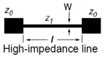
(1)As per the above formula, I can find what is the required length of the line for that particular inductor value. Anyone knows the same kind of formula for CPW line? And how do I know what should be the charateristic impedanced of the line, are there any conditions or procedures to choose it?.
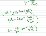
(2)But as per below formulas also we can get inductance.
stub.JPG

I know that (2) can be used while doing stub matching but we can also use (1) for matching, however it is just the substitutuon of inductor. I want to know which one to use when and any more insight on this. Thanks.
 
Last edited:

Anyone knows the same kind of formula for CPW ]line?
It is same.

And how do I know what should be the charateristic impedanced of the line,
Use transimission line calculator which supports CPW.

I know that (2) can be used while doing stub matching
but we can also use (1) for matching,
They are all same.
Learn and understand very basic things surely.

Consider how to realize short.
Simply if it is difficult to realize short, short stub is not chosen.

If you use laser trimming, you have no option except for open stub.

Learn actual measurement not EDA Tool Play.
 
Last edited:

CPW cannot be used for Inductor Realizations.Especially if the frequency is not sufficiently high, making an inductor by using Transmission Lines is not practical at all..
 

The simplest microstrip inductor would be from a microstrip line without ground (the ground decrease somehow its inductance).

The inductance of an isolated (no groundplane), high impedance microstrip line (W << W(Zo)) is given approximately by:

L(nH/mm) = 0.2*{ln[l/(W+t)]+1.193+0.2235(W+t)/l}

where W is the width of the strip line, t is the metal thickness, and l is length.
 

Attachments

  • line.gif
    line.gif
    4.4 KB · Views: 194

CPW stands for co-planar waveguides. Transmission lines can be realized on-chip using co-planar metals as Ground-Signal-Ground configuration. It can also be realized by routing the signal trace on a different metal layer and ground on a different metal layer. Then its no longer CPW.

How to choose Z0?

Increasing Zo will mean that you get the same inductance for a shorter length of line --> lesser losses. Also, the bandwidth of matching using transmission lines increases when the impedance to be matched and the characteristic impedance are close to each other. Its an iterative process to get it right.

I also hope you realize that the first expression comes directly from the algebraic manipulation of a shorted stub.
 

Attachments

  • Capture.JPG
    Capture.JPG
    45.9 KB · Views: 191

Status
Not open for further replies.

Part and Inventory Search

Welcome to EDABoard.com

Sponsor

Back
Top