Continue to Site

Welcome to EDAboard.com

Welcome to our site! EDAboard.com is an international Electronics Discussion Forum focused on EDA software, circuits, schematics, books, theory, papers, asic, pld, 8051, DSP, Network, RF, Analog Design, PCB, Service Manuals... and a whole lot more! To participate you need to register. Registration is free. Click here to register now.

Strategy for a multi signal generator using a MAX10

Status
Not open for further replies.

Pastel

Member level 3
Joined
Jun 30, 2019
Messages
55
Helped
2
Reputation
4
Reaction score
1
Trophy points
8
Activity points
969
Hello!


As explained in another post, I'm trying to make a multichannel signal generator.
At the moment, it works fine with sine waves, which is quite boring, but at least
it works. The previous problems were how to use the on-chip RAM, and thanks to your
help, I could use it, it was a matter of setting the right option.

Now I have 2 signals, but I want more (about 8). In this case, I have to instantiate
4 ROMs, but I found no other solution than using the same module 4 times, and the
problem is that it loads the same data. Although it's not the case, if I want to make
a 8 channel sine wave, it's quite silly to store the same data at 4 different places.

What would be the right strategy to continue?
I was thinking about :
1. Storing only 1/4 of the wave in every dual port ROM instance. So it would save
3/4 of the space, so if I use 4, it's stil silly because I store 4 times the quarter
wave, but at least it saves space. BUT: in this case I can't use the on chip RAM because
it expects the data to be thrown unconditionally, and I just made a test by unfolding
the quarter sine wave. I tried, it works, it makes a sine wave from a quarter of a
sine wave, but no internal RAM is used, RAM Can't be used, apparenlty.
// ROM must be read unconditionally to infer dual port ROM

2. Storing the wave to user flash.
I don't know how to do that, but before trying it, I would like to know if I can
access it as fast as the RAM (i.e. at 50MSpl/s). If I can, then it would be an option.
Question: would the flash be fast enough to throw samples at 50Msps?

3. Storing a full sinewave (which therefore enables to use the RAM), but with less
samples. For instance 1024. Then with an interpolation by a power of 2 (very fast),
I should be able to get the job done fast enough.
Question: can an interpolation be done at every cycle?
For example if I interpolate by N (which is a power of 2), I would use an accumulator
acc with N more bits than my data. Then a sample between data and data[i+1] at a istance
k from data (0 < k < N), then I would calculate acc <= k * data + (N-k) data[i+1]
and then finally DA <= acc[WID+N-1:N].
Does this make sense?

Any hint or comment? Another strategy?

Pastel
 

Hello!

You're right. Sorry. I was referring to this discussion.

In the meantime, I made error calculations to estimate what would be a reasonable amount of lookup table to
store a sine wave. In fact, that's a lot less than I thought.
I thought (naively) that if I want to generate a sinewave from a table, I would need maybe 64k samples
and therefore I wanted first to use on chip memory.
In fact it can be done by interpolatiing a smaller array. I made calculation with 1k samples of 20 bit data,
and I found out that the ratio error / amplitude would be 0.000008 or 8ppm. So if I use a 1k samples
array, use linear interpolation and truncate the result, there is a high chance that I will get a decent quality
signal. I'm trying the verilog part of this method right now. The next step will be a 8 port memory.
Not possible to use the on-chip memory in this case, but hey, with only 1K array, it looks like it
will be economical, possibly scaling down to a smaller device.

Now if anybody has hints on how to use internal flash to store tables, it may also help.

Thanks,

Pastel
 

As mentioned by betwixt, always link related threads https://www.edaboard.com/showthread.php?385832-How-to-instantiate-a-submodule-in-Verilog

1.
I tried, it works, it makes a sine wave from a quarter of a
sine wave, but no internal RAM is used, RAM Can't be used, apparently.
Partial RAM tables (e.g. quarter wave) can be used, you need to learn the prerequisites of RAM/ROM inference. Your code is probably not complying with the RAM/ROM design templates.

If you have difficulties to understand it, instantiate dual port ROM directly through IP catalog. It gives only access to the hardware options that are available in FPGA.

2. No. At the hardware level, user flash is read bit serially -> too slow.

3. Coarse tables with linear interpolation are a frequently used option. Unfortunately you need to access to consecutive table values for one interpolated value. Thus either both ports of the dual port ROM or two clock cycles are required for one interpolated sample.

To learn about the options of multi-channel signal generators, evaluate the NCO IP core. Although it's not available for final design in the Quartus Lite edition, you can compare the signal quality and speed of various topologies.

Even without actually instantiating NCO IP for test, just studying the manual can give you many insights.

RAM blocks can run in C8 speed grade up to 200 or even 250 MHz. If your sample rate is 50 MS/s, a mux ratio of 4:1 is feasible. However, utilizing FPGAs to the speed limits isn't particularly a beginners project, it's probably better to start with more basic solutions.
 

Hello!

Thanks for your reply!

3. Coarse tables with linear interpolation are a frequently used option. Unfortunately you need to access to consecutive
table values for one interpolated value.

Yes, that's what I just found out. I'm thinking of using a dual port RAM as if it was a single one, and therefore hope to
have access to 2 samples on the same cycle. For this project, I want to keep within my understanding range. If it works,
then I will think of other options. I'm aware it might not be the missionary position of FPGA programming, but
I will explore other options when it starts working.

Even without actually instantiating NCO IP for test, just studying the manual can give you many insights.

That's what I'm trying to do. I'm not against reading documentation, but as a beginner, it's a bit like reading Kant,
Hegel or Schopenhauer at the elementary school. When I learned C, I had the K&R book, but if I had fully read it before
starting programming, I would have been unable to write a single program. So this will be a parallel work...

Pastel
 

Hello everybody!

Just to keep you informed. I have tested one of the 3 strategies I was thinking about (the 3rd one,
using shorter wave sets with double access ram, and interpolate the results).
I'm impressed! Even with 64 samples waves, I get an incredible quality, as shown below.
So basically what I do:

- I store a wave using one of Quartus templates. If there are other beginners here, right click
in the editor window, and choose:
Insert Template -> Verilog HDL -> Full designs -> RAMs and ROMs -> Dual port ROM.
Edit what you got to give it the right dimensions. In my case, I am using 20 bit data to have
some extra bits in case of rounding.

- Another trick to make it work is the configuration allowing to use RAM on a MAX 10:
Go to Quartus' top menu.
Assignments -> Device -> Device and pin options
In menu Configuration mode, choose Single uncompressed image with memory initialization (512kbits UFM).

- I built an interpolator implementing one dual port ROM. But I get rom[address] and rom[address+1]
and I calculate from these two values.

As for the result scope screen copy, the yellow curve shows the signal before interpolation, where you
can clearly see the 64 levels. And the blue curve is the yellow curve in which you would add small
triangles to get rid of the stairs.

- The FFT window is a FFT of the blue curve. I'm surprised that such a low noise level can be reached.

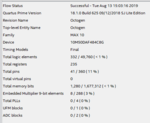
- The gray image shows the compilation results. 1280 bits of memory used. (64 * 20-bit).

NB: I had many problems with wires vs regs, so I remembered one of the first posts. I think it was
from Fvm who said that it compiles perfectly in system verilog. So this time I used a .sv file and
it's a lot better, the compiler stopped nagging about details and I don't need any wire in the whole
program.

About the compilation results:
CompileResults.PNG
This FPGA looks incredibly powerful. I made a single signal for the timebeing, but it uses lessthan 1%
of the assets except for the pins (I have a MAX5875 wired, 2 16-bit ports + control signals and a few
LEDs).


Then the scope picture which shows how smooth a 64 sample sine wave can become using a plain
linear interpolation.

I also tried with 1k Samples, in which case it takes 20k (about 1% of the total memory per signal).
But the 2 curves look the same, so it's less impressive.

PA_001.png

That's it for today! Many thanks for your cooperation!

Pastel
 
  • Like
Reactions: FvM

    FvM

    Points: 2
    Helpful Answer Positive Rating
NB: I had many problems with wires vs regs, so I remembered one of the first posts. I think it was
from Fvm who said that it compiles perfectly in system verilog. So this time I used a .sv file and
it's a lot better, the compiler stopped nagging about details and I don't need any wire in the whole
program.
This is the wrong way to "fix" the wires vs regs. It will result in warnings in a language compliant simulator as reg is not the same as wire even in Systemverilog. It seems to me that Quartus is taking the allowed usage of logic and making reg the behave exactly the same way, which is incorrect. logic can be used in places where it can be like reg or like wire as "wire logic" or logic for short.

I mentioned before that Modelsim (a Systemverilog compliant simulator) does issue an annoying warning about the incorrect usage of reg (where a wire should be used) whereas in Verilog mode it errors. It appears that Quartus synthesis doesn't even warn you it just lets you use a reg. I'm pretty sure not all synthesis tools will allow this and I'd be worried that in some situations you might end up with a simulation synthesis mismatch. Of course you've never mentioned doing any kind of simulation.

You should read 2.3 Variable types in this paper and read the Recommendation at the end of that section.
 

Hello!

Thanks for your advice.
I'm aware I may be doing a lot of things the wrong way, but that's the point: I'm doing things and
I get them working.
I don't know exactly how high I score on the scale of speed of learning, but within a month I could
develop something and it works reasonably well, even if it will never be a product, just learning material.
I made a small PCB which is mostly wrong and full of patches, but I get signals from the DAC at a high
sample rate, which would be clearly impossible with a microcontroller.

Next step, create a SPI slave object that will receive control data from a microcontroller. And mayb
first fix this clock problem (I was told I should use a PLL instead of making the DAC clock myself).

Learning methods like "you'll ride a bicycle when you know how to ride" don't work. I have to ride and
possibly fall a few times.

My way of learning may sound cahotic (actually it is), but getting info from many sources helps a
lot, and the info I got on this forum probably saved me hours or even days of bumping against a wall.

Pastel
 

Synthesis tools and simulators have surely to problem to recognize the purpose of false Verilog regs used as wire, they do the same when processing VHDL code which uses signal in both roles.

But I nevertheless agree with ads-ee. If you decide for Verilog or Systemverilog, you should learn soon the expected syntax that doesn't bring up confusing warnings.
 

Hello!

you should learn soon the expected syntax that doesn't bring up confusing warnings.

I think it will happen gradually and naturally.

Now I don't even fully understand the FPGA related vocabulary. It doesn't mean that I have
to learn it first. For instance, I'm not even sure of what synthesis, simulation, verification all
mean. I know I'm doing synthesis because there is a synthesis progressbar. From the name
itself, I guess it means something like compiling the verilog code and transform it into a design,
fit the design into the FPGA, but there might be other subtleties I don't understand.

Verification? Yes, I verify what I do with an oscilloscope, but I think there is another meaning.
The paper linked by ads-ee talks about the myth of system verilog as a verification language.
So verification has something to do with language, but let's be frank, I don't know what it
is, and I don't feel the need for it right now because I operate exactly like for microprocessors.
- Edit a program
- Compile it
- Plug the emulator (or whatever is is, the USB blaster for Altera)
- Load and run
- Observe the results on the scope.

Maybe it works for the time being because I'm using 1% of the FPGA, and maybe I will run
into trouble when the source expands, but as long as it works, I will probably not feel the need
to change my method.

Note that I'm not especially proud of not knowing what verification is, it's just a fact: for the
time being, I don't know. And I'm sure I will know more by programming, trying, correcting, etc...

OK, back to development of my home brew SPI engine...

Pastel
 

Verification? Yes, I verify what I do with an oscilloscope, but I think there is another meaning.
You perform verification of the design before you build a physical version of it. What you are doing is testing unverified code on hardware.

If you were going to build an ASIC from Verilog like you do now you would go out of business even if you have more money than Bill Gates, Jeff Bezos, Mark Zuckerberg, Larry Ellison, etc. Every time you have to spin the design due to a latent bug you did not discover by "code inspection" means another mask charge of multiple millions of dollars.

The paper linked by ads-ee talks about the myth of system verilog as a verification language.
Should read as "the myth of system verilog as being a verification only language."

So verification has something to do with language, but let's be frank, I don't know what it
is, and I don't feel the need for it right now because I operate exactly like for microprocessors.
- Edit a program
- Compile it
- Plug the emulator (or whatever is is, the USB blaster for Altera)
- Load and run
- Observe the results on the scope.
Verification has nothing to do with language it has to do with proving you did a design that meets the requirements and performs all of its intended functions, before you create a physical copy of it. That is why verification languages exist, to build test code to exercise your design before you build it.

Your current methodology only lends itself to the simplest of designs. Complex designs if done using your methodology are destined to fail. Seen it happen many times with "engineers" who don't do any engineering but just thrash around slapping code together and making it pass synthesis, putting it on a board and trying to debug through the equivalent of a straw (32-signals to a logic analyzer out of 100,000 signals in the design).

Maybe it works for the time being because I'm using 1% of the FPGA, and maybe I will run into trouble when the source expands, but as long as it works, I will probably not feel the need to change my method.
Fine put your blinders on, but I'm sure you will regret developing those bad methodology habits in the long run. IMO it is better to develop good habits early so you don't have to change those habits later (which is much harder to do).
 

Status
Not open for further replies.

Part and Inventory Search

Welcome to EDABoard.com

Sponsor

Back
Top