Continue to Site

Welcome to EDAboard.com

Welcome to our site! EDAboard.com is an international Electronics Discussion Forum focused on EDA software, circuits, schematics, books, theory, papers, asic, pld, 8051, DSP, Network, RF, Analog Design, PCB, Service Manuals... and a whole lot more! To participate you need to register. Registration is free. Click here to register now.

[SOLVED] Failing to program ALTERA Max 7000A

Status
Not open for further replies.

andrew_que

Junior Member level 2
Joined
Dec 1, 2015
Messages
22
Helped
0
Reputation
0
Reaction score
0
Trophy points
1
Activity points
276
Hello everyone.
I recently bought a bunch of Altera MAX 7000A CPLDs on RS components in the plcc44 package.
I already have at home one of those cheap clones altera usb blaster with JTAG output.
I tried a simple breadboard setup to program the cpld with altera quartus without success.

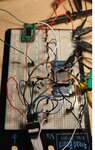
First, the only useful information about programming in the CPLD datasheet is that it complies to the "industry-standard 4-pin IEEE Std. 1149.1" interface, which would be TDI,TDO,TMS,TCK. Now I found all those pins on my CPLD pinout. I'm providing 3.3V to one VCC pin of the CPLD and using common ground for my PSU, CPLD and USB Blaster JTAG. I've also found the pinout of the JTAG connector from the USB blaster. There are 10 pins but 3 of them are NC and one is a doubled GND. The first attached figure shows how I wired it all (I found the pullup/down res configuration from the schematic of the chinese FPGA devboard where my usb blaster came from). Quartus doesen't recognize my cpld. I'm sure my quartus (ver II 13.0) has support to the device because I got to choose it during the new project wizard. Actually, in the software I selected EPM7032AELC44-10 whereas mine has an additional N at the end, though I don't think this can make a difference.

I have tried changing USB port (3.0 and a 1.0 in the front panel, and a 3.0 in the back panel directly connected to the mobo). I have tried changing the USB cable. So I went ahead and hooked up my DSO to the four JTAG pins and got some waveforms obtained while trying to get quartus recognize my cpld (Auto Detect button, second attached figure). The third figure gives an overall of the process. Now, I'm not an expert of jtag but it looks quite strange that TCLK would not tick while data is sent throught TDI. Also, fourth figure shows a detail of TCK in the final portion of the waveform and to me it looks a bit odd that they would go with 90%ish duty cycle... Is it possible that my usb blaster is fried? I used it so little and always kept it inside its box, never exposing to heat/water, also I opened it and it looks fine. Maybe I'm using the wrong pin, I'm using a picture found online as reference (fifth attached figure)

Do you have any suggestions? I really thought this would have been easier... but now I'm engaged to try and solve this.

attached figures
Schematic:
1.png
Quartus recognizes USB BLASTER but fails to recognize CPLD:
2.png
JTAG Scan process measurements:
3.png
TCK detail after the TDI run:
4.png
USB BLASTER pinout reference:
5.jpg
 

Did you connect all four VCC and all four GND pins on the MAX 7032? You only show two pins on your schematic.

The fact that the tool says it doesn't find a device on the chain indicates the MAX isn't on the chain. Either it isn't powered or the JTAG connections are wrong. Your schematic doesn't tell us if you even wired the parts up correctly on your breadboard.

You also don't show any bypass caps in your schematic, which you will probably need when and if it starts programming. You will probably want both a bulk and high frequency caps on each VCC pin. Without looking at the datasheet in detail erasing and programming the eeprom cells in the device probably draws more power. Someone who has used these devices might have more experience with what is required (I'm only giving general advice).
 

Hello all, thanks for the replies
@ads_ee:
- I did connect only one VCC and one GND. I have fixed this and also added bypass caps and a pullup resistor
- Sorry you are right, I have updated my schematics to fully show my breadboard connections. Only one note, where eagle part shows pin 3 is PD/VCC, the cpld datasheet only says VCC
@akanimo
- Thank you for the link, I slightly modified my schematic to have the same exact circuit (added pull up resistor and a new connection to the jtag header, even if my specs say it is not connected in the usb blaster). The only difference is that I don't have an oscillator for the CPLD but he clearly states it's not used for programming but only an additional general purpose feature.
- There is nothing behind the popups, completely blank screen
Here is the updated schematics:
schematic2.PNG
needless to say the problem persisted, quartus gives the same messages
 

TDO stays suspiciously quite during clock pulses although it should be tri-stated as long as the JTAG interface isn't responding. Could it be shorted to ground? Check with a multimeter.

I presume you have bought new, not used MAX7000A. Otherwise there's a certain risk that the JTAG interface has been disabled. An option to gain additional logic pins, for compatibility with old non-JTAG MAX7000. If so, JTAG can be only re-enabled with Altera MPU (or possibly some third party parallel programmers).

- - - Updated - - -

P.S. In your recent schematic, you have placed a pull-up at TDO, although not suggested by Altera. TDO should not stay a 0V then. Either shorted or some other defect. Can you check TDO level with USB Blaster disconnected?
 

Can you show a picture of your JTAG header?
 

@FvM:
- I checked with a multimeter both TDI and TDO impedance to ground in all possible configuration of JTAG and VCC connected/disconnected, always getting high impedance.
- Yes i bought new CPLDs (from RS components online distributor)
- TDO @ 0V was indeed in my previous configuration, now with the pullup it goes high.
So
I removed the pullup from TDO and, guess what.. stuff happens! I can see the TCLK signal from USB BLASTER to actually tick during TDI, which makes quartus recognize something, albeit totally wrong..
At this point I believe the next step should be try and make something more stable with a perfboard because this is really getting a mess and I have the feeling that just the shadow of my arm moving above it is producing differences.. gosh do I hate prototyping

@akanimo picture of the usb blaster with JTAG interface. The pin header reference I'm using should be correct (see in open post, last picture attached) as it's the same
found in other sources like your hackaday post.
usb-blaster.jpg
Here is what happens in quartus. AutoDetect still popups the same warning but when I run the JTAG tests i get this:
detection_screen.png
p.s. See how it believes TDI is grounded even though my measurements contradicts it and even the oscilloscope is getting TDI signal
 

I won't overrate the detail results. TDO stays apparently tri-stated and the USB-Blaster is picking up some noise, interpreted as meaningless JTAG data.

If the MAX7000 wiring is correct and the device receives meaningful JTAG commands, the chain would be recognized and ID read. Besides incorrect connection, your "USB Blaster" (actually a Chinese clone of the original Altera/Intel programming adapter) may be defective and send somehow incorrect signals.

I would check if the very first TAP controller commands (TCK and TMS toggling) are output correctly.

Also cross-check correct operation of the USB Blaster with a different Altera device.

- - - Updated - - -

The TCK detail waveform screenshot shows a clock fall time of about 1 us. That's rather slow and not expectable for correctly working TCK driver. I wonder if other parts of the JTAG transaction show reasonable clock fall time.
 

You just showed the USB Blaster in post #7 instead of the header. If you do not have a header then it's possible you may have flipped some pins by mistake. You may have to confirm this again.

- - - Updated - - -

Maybe you should delete the programming file you have on the programmer GUI and then click on "Add File" and select the programming file and try again.

- - - Updated - - -

Also, reconfirm the model number on the chip and the device you selected on Quartus.
 

According to post #1, the OP is performing an autodetect. It will recognize MAX3000/MAX7000, asking the user for selection of the appropriate device. In so far it's not necessary to select a device in advance.

Flipped header pins may happen, but I have no idea how you want detect it from a photo. We would need to see the complete header to device wiring.
 

@FvM
- Yeah usb blaster waveforms look very suspicious. I knew it is a chinese ripoff. It came with a cyclone IV chinese devboard, bought about 2 years ago, almost never used.
The thing is I could program correctly the fpga, but now that i try again I get the same error so..
very probably the cause is this usb blaster, but its so lame I did really almost never use it and kept with care...
Besides how can it break this easily its not that many components, on top of that they are good quality: got an atmel mcu and a texas insruments something, maybe a JTAG controller. soldering looks fine too. A couple capacitors look a little darker though, and they measure about 500 ohms across, so maybe if I find the schematic i could check if that is correct. By the way now that I'm trying it opened up I can see I can make the led light brighter if i push the usb cable harder :laugh:
If I have to buy another one, would you suggest me getting another clone or maybe the original thing?
@Akanimo,FvM
- I didn't show the header because its just a mess of jumpers, you can trust that i followed the pin reference in post1 and schematic of my second post. I'll attach a pic of the circuit if you're curious just how messy it is and why i'd like to proceed with perfboard
@Akanimo
- confirmed, same device number, just my cpld has that additional final N. Also tried creating new jtag chain file and new project
full circuit:
breadboard.jpg
usb blaster:
blaster.png

-- update --
added overlay to breadboard pic with paint
 

Attachments

  • breadboard.jpg
    breadboard.jpg
    96.1 KB · Views: 223
Last edited:

The board you are using, it is PLCC44 to DIP-what? Is it PLCC44 to DIP44 or PLCC44 to DIP40?

That red wire connected to the JTAG connector doesn't look cool.
 
Last edited:

You have fine eyes, It is PLCC44 to DIP40.
Of the 4 pin missing, 2 were GND and VCC. To overcome this I "implanted" the leg of a resistor in the right places, thin enough to get stuck firmly. Checked continuity also to neighbouring pins, it is fine
Also the red wire is fine and dandy - just to be sure I replaced it with my last jumper ( I didn't think i had more) but nothing
 
Last edited:

It's not very clear how you made the connections to the DIP40 board. The missing pins may be Vcc and GND but the connections from the pins of the DIP40 board to the pins of the PLCC socket are not the same as those from DIP44 boards.

Do you have a schematic of the DIP40 board that you can show to us?
 

I got that breakout board from another piece of equipment I bought some time ago - a 40 pin flash/eeprom universal programmer.
Indeed it is not the same as a regular dip44, unfortunately I don't have a schematic and I had to probe each pin with a multimeter to find where to connect stuff.
I repeated this operation several times to be sure everything was right
Anyway I don't like this setup. There are so many things that could go wrong, like bad contact of jumpers and misconnections, that even with the most attention the probability of something being wrong is still high. On monday I'll go get some perfobards and try to get a better setup.
 

The JTAG cable connection in photo "full circuit"doesn't look right. TCK should be at pin 1, the red marked flat cable wire.

As for the questionable PLC44 to DIP40 mapping, to you have a datasheet or type name of the adapter board?

That's how autodetect with correctly connected MAX7000 device looks like, signals are TCK, TMS, TDI, TDO, top to bottom.

Autodetect_MAX7256A.png

The TMS sequence is TAP_RESET, DR_CAPTURE (ID-code), DR_SHIFT. At this point, TDO is enabled. ID-code is shifted out, followed by a test sequence shifted in at TDI in the meantime to measure the chain length.
 
I looked for the datasheet of that breakout board but no results.
The board reads this:
PLCC44-DIP40
78E/89C
51/52/58
SERCOND.
Anyway according to altera datasheet TCK goes to pin 32.
Cattura.PNG
Thank you for your measurements. I didn't know about TMS sequence, thought it was just an active low enable signal.
Anyway the fact that i was measuring directly the output of my usb blaster with DSO and looking how different it is is convincing me that the usb blaster is the culprit.
edit:
WAIT a minute, according to the reference pinout pic I posted in the first post the red line would be TDI, but in my flat cable I even have a trinagle in the black plastic ending
of the cable which usually points to pin 1 which should be TCK instead. Also looking at the waveforms TDI does look like a clock... I'll try flipping the connections thanks.. too bad that i disassembled everything ten minutes ago

- - - Updated - - -

So I'm happily declaring victory, the problem was indeed the pin row was swapped.
That black indicator in the pinout picture reference fooled me. Now this means that the broken part is not the usbblaster but instead the fpga devboard :( it pains my heart
Thank you all!
As a bonus, i took my time to rebuild it a little bit cleaner
final_breadboard.jpg
 
Last edited:

The adapter board is for 89c51 uC family, pin assignment is identical to original Intel 8751 in PLCC44 package. The four center pins are unconnected, respectively the DIL pin numbers are increasingly shifted. Seems to be correctly accounted in latest breadboard wiring.

VCC Pin23 can't be accessed by the adapter, should solder a wire to the adapter.
 
Thanks
Indeed pin 23 and pin 10 need a robust connection. For testing, I used the "resistor leg" technique. Now that I know how to make it work I will make a pcb similar to the one in the link posted by Akanimo.
 

I didn't know about TMS sequence, thought it was just an active low enable signal.
Test Mode Select (TMS) causes the TAP FSM transistions. The FSM diagram in the second image in post #7 shows the TAP FSM with the 1s and 0s being the TMS value to transition to that state.
 

Status
Not open for further replies.

Part and Inventory Search

Welcome to EDABoard.com

Sponsor

Back
Top