eengr
Member level 4
Hi
I am trying to understand the behaviour of Human Body Model simulation circuit in Tina TI.
I found a circuit provided by TI (as below)
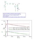
I ran a transient analysis of this and got the curves as shown in the graph above (for Vout & AM1)
The way I understand is: that Human body side is modelled as 100pF Capacitor with some initial charge of 2kV. & it discharges through 1500 resistor.
What I am struggling to understand is that during this transient analysis how is this Switch SW1 behaving? (I can see the SW1 open but I still see the Current & voltage waveforms)
What is the purpose of L1 here?
Are C22 & R2 representing any random load?
I have done another transient analysis (this time probing Vin aswell)
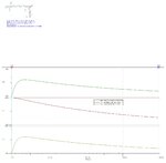
So, it looks like Vin (Charge across 100pF) is decaying down with time but still don't know how!? In order for it to decay somehow the switch needs to connect it to the node of 'L1' but when and how is that happening?
- - - Updated - - -

Ok I think I found the answer to the question related to 'Switch'. It looks like SW1 is Time-Controlled Switch & it is set ti turn ON at t= 0sec & OFF at t= 1sec
So only help I need is the reason for L1 & if C2 & R2 are some random load?
I am trying to understand the behaviour of Human Body Model simulation circuit in Tina TI.
I found a circuit provided by TI (as below)

I ran a transient analysis of this and got the curves as shown in the graph above (for Vout & AM1)
The way I understand is: that Human body side is modelled as 100pF Capacitor with some initial charge of 2kV. & it discharges through 1500 resistor.
What I am struggling to understand is that during this transient analysis how is this Switch SW1 behaving? (I can see the SW1 open but I still see the Current & voltage waveforms)
What is the purpose of L1 here?
Are C22 & R2 representing any random load?
I have done another transient analysis (this time probing Vin aswell)

So, it looks like Vin (Charge across 100pF) is decaying down with time but still don't know how!? In order for it to decay somehow the switch needs to connect it to the node of 'L1' but when and how is that happening?
- - - Updated - - -

So, it looks like Vin (Charge across 100pF) is decaying down with time but still don't know how!? In order for it to decay somehow the switch needs to connect it to the node of 'L1' but when and how is that happening?
Ok I think I found the answer to the question related to 'Switch'. It looks like SW1 is Time-Controlled Switch & it is set ti turn ON at t= 0sec & OFF at t= 1sec
So only help I need is the reason for L1 & if C2 & R2 are some random load?
