Continue to Site

Welcome to EDAboard.com

Welcome to our site! EDAboard.com is an international Electronics Discussion Forum focused on EDA software, circuits, schematics, books, theory, papers, asic, pld, 8051, DSP, Network, RF, Analog Design, PCB, Service Manuals... and a whole lot more! To participate you need to register. Registration is free. Click here to register now.

About Separating Supplies on PCB.

Status
Not open for further replies.

Pastel

Member level 3
Joined
Jun 30, 2019
Messages
55
Helped
2
Reputation
4
Reaction score
1
Trophy points
8
Activity points
969
Hello!


I'm not sure this is the proper place for that kind of question, so if it's not,
@moderators: please feel free to move this post.
I have made my first FPGA design. I'm using a MAX10 board and an extension on which
I have set a DAC (MAX5875).

For the moment, all my design does is generating a sine wave from an array (everything
is explained in the FPGA section).
Now what happens is that the SN ratio is quite poor. I get around 70 dB.
As the DAC is 16 bit, it's 96 dB on paper, and according to the datasheet, it should
be greater than 80 dB SFRD. So maybe it's the proper time to design a new PCB.
What I did (it's my first DAC hardware) is putting all grounds together, all
power lines together (of course the 1.8 and 3.3 are separated).

Now is it better to separate grounds? I have read contradictory stories about this,
and some are saying that a solid ground plane is better.
I made a 4 layers PCB. Front, L2, L3, Back. L2 is only ground. L3 is only power,
+5V, +3V3 and +1.8 V in the proper areas.
So here are my questions:

1. Should I separate grounds? (It might be a little bit tricky, I have more than 1 DAC,
so the story of 1 single contact point between AGND and DGND is not easy, there would
be islands of DGND and other islands of AGND. Ok, having a single point, then thick
lines leaving from there is possible. Another solution would be to add one AGND plane.
Would this make sense?

2. Should I separate DVCC and AVCC? If yes, I was thinking about these solutions:
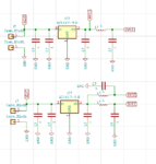
Circuits.PNG

In the first case, on top, is it better to have AVCC at the output of the regulator, or would
it be better to do the opposite?
Would the second solution be better?

Thanks for any hint.

Pastel
 
Last edited:

Hi,

Now is it better to separate grounds? I have read contradictory stories
..it depends ..., thus you read contradictory stories.

Voltage noise = current noise x impedance

Thus you have to find out
* who causes the current noise
* and what path takes this current

In best case it's just your noise measurement (equippment) that causes the current .... and you just need to connect the GND at another place.
If possible do the noise measurement and make a frequency plot (FFT). Then you are able to analyze the source of the problem.
(Maybe mains frequency and overtones of an Earth loop, or 200kHz of an SMPS)

Separating power supplies is useful when you expect the digital supply to be noisy.
Separating Grounds is useful when you expect the Ground to be noisy ... caused by high noise current through a Ground section.

In most cases - reducing the noise you talk about - can not be done at the schematic but in the PCB layout and wiring.

Thus the information of your post#1 is not sufficient. We need to know about wiring (especially analog signals and Grounds). We need to detect loops ... even Earth loops. Upload photos of your complete circuit and photos of detail circuits.

Klaus
 

In mixed signal design with multiple analog and digital functions, there's no reasonable way to use separate analog and digital grounds. A continuous common ground plane is the usual solution. Separate power supplies may be helpful, but more important to bypass the power supplies near each mixed signal device.

The key for good SNR with devices like MAX5875 is utilization of the differential analog output signals. I'm not even sure if power supply is your primary problem.
 

Hello!

Thanks for your replies.

In mixed signal design with multiple analog and digital functions, there's no reasonable way to use separate analog
and digital grounds. A continuous common ground plane is the usual solution.

OK, that's a good start point. On top of that, Klaus was saying that voltage noise is current noise x impedance, so if
I get a solid plane, the impedance will be minimal and therefore noise minimal.

but more important to bypass the power supplies near each mixed signal device.

Sorry, I'm not used to the hardware vocabulary. What do you mean by bypass? I know (more or less) what is a bypass
cap, but as a rule any chip has bypass caps, so is there anything else to do? Other caps to set somewhere?

The key for good SNR with devices like MAX5875 is utilization of the differential analog output signals. I'm not even
sure if power supply is your primary problem.

I didn't reinvent the wheel, I'm just using fig. 7 of MAX5875 datasheet. I'm using the 3 resistors as explained,
(well, I'm using 24 and 51 ohms instead of 25 and 50), and I'm measuring outP and outN, then substract and do
an FFT on the output. Unfortunately I don't have a differential probe. But I will make one converter today (a kind
of poor (wo)man's diff probe) to watch what happens.

Anyway for my next PCB:

The MAX10 board I am using is this one.
There are many grounds spread over the 2 connectors, so I will keep one single group of grounds on one of the
connectors. Not sure if will change anything, but at least there will be a single ground between 2 boards.

I will use separate power lines for analog and digital supplies.

I will add a differential to single end output amp, just for test (I have a few TI's 4521).

I will add power supply on the analog board, not use the FPGA board's supply which is really noisy.

And as I want a differential output, I will also add differential amps. Maybe the same with jumpers, one single end
test mode and one differential output mode.

By the way, for my voltage regulators, I think of using regular (linear) devices because I don't want to have to fight
against switching noise. But are are there some better than others? What should I check first? I need 5V, 3.3V, 1.8V.
Right now I'm using a lab external supply and all currents are in the 50 ~ 100 mA range. But as my FPGA design
gets bigger, I guess the current will increase. How should I choose? With PSRR?

Thanks for any comment.

Pastel
 

Hi,

and I'm measuring outP and outN, then substract and do
an FFT on the output. Unfortunately I don't have a differential probe.
Measuring outN and outP at different time will not give useful noise result.

Klaus
 

Hello!

Measuring outN and outP at different time will not give useful noise result.

I'm not sure of what you mean by different time. I am hooking my scope's ch1 and ch2 on outp and outn,
then use a math function of the scope to calculate the difference, so on the math channel, I get outp-outn.
So I don't measure them at different times.
I don't know exactly how and why it could have more noise than with a differential probe, but at least
the results are slightly better than on ch1 only or ch2 only. Maybe because there is some common noise
between both channels, which cancels nicely. And also because I have twice the amplitude.

Pastel
 

Hi,

Maybe because there is some common noise
between both channels, which cancels nicely. And also because I have twice the amplitude.
That's the idea behind different signalling.

Klaus
 

Note the MAX5875 Eval board used three PCB ground sections: AGND, DGND, CLKGND. Maxim also used DAC output common-mode chokes and output transformer.
 

Hello!

Thanks for your reply. OK, that's a good input. In the meantime, I have made measurements, and also
a comparison between a Tek signal generator and the hardware I made.
NB: I'm comparing OUTP of the DAC with Tek's output (single ended).
Tek is the red FFT at the bottom, my generator is on top, purple curve.
The first harmonic is better with what I made, so although there might be a lot of room for improvement,
I have the feeling it's not that bad with my hardware full of patches.
On the next PCB, I will add a proper diff -> single end conversion, although the purpose of this experiment
is to make a differential generator.
NB: OutN is not used (light blue signal).

Thanks for all your comments and advices.

Pastel

PW_009.png
 

Note the MAX5875 Eval board used three PCB ground sections: AGND, DGND, CLKGND.
Yes it has. This kind of design works fine for evaluation circuits with one and only one mixed signal device. It's not feasible for most real world designs. Other design details of this board can be nevertheless implemented.
 

Status
Not open for further replies.

Similar threads

Part and Inventory Search

Welcome to EDABoard.com

Sponsor

Back
Top