Continue to Site

Welcome to EDAboard.com

Welcome to our site! EDAboard.com is an international Electronics Discussion Forum focused on EDA software, circuits, schematics, books, theory, papers, asic, pld, 8051, DSP, Network, RF, Analog Design, PCB, Service Manuals... and a whole lot more! To participate you need to register. Registration is free. Click here to register now.

Voltage sharing for IGBT's in series

Status
Not open for further replies.
Hi Easy peasy and FvM.

Thank you for your valuable input.

First let answer the question of how the drivers are isolated. All the drivers and the MCU are all powered from individual secondary windings on a toroid transformer.

The test situation is as follows. All IGBT's are OFF and stay OFF the entire time until I press a button which results in a single 500uS gate signal on all drivers. For this test I'm NOT pressing the button, just trying to crank up the HV.

Now if I just crank up until the power supply stops responding to me turning the knob, everything survives. So we have a situation where the power supply's can't deliver more current than it's designed for in this case up to 40mA, so where does these 40mA go? I measured 1mA through the entire stack, which makes the resistors hot to the touch. So I'm thinking if the reminding current is lost in the stack, I would surely hear, see and smell it.

In the next test I crank up until the power supply stops responding to me turning the knob, then I turn the knob back a little bit until voltage starts dropping. Then I press the button and turn all IGBT's ON - everything works just fine.

So what I'm trying to say is that it is hard for me to believe it's a breakdown of the drivers isolation barrier. During this testing I haven't blown up a single driver, only the IGBT's.
 

how do you know, for sure, you haven't damaged any of the driver chips? if they are in series on the G-E - and the input is ground referenced - then 3kV will surely break down some of them - a complete schematic would help clarify matters ...
 

how do you know, for sure, you haven't damaged any of the driver chips?

I don't know anything for sure. I can just make the assumption based on the fact that the IGBT's turn ON and start conducting for 500uS.

if they are in series on the G-E - and the input is ground referenced - then 3kV will surely break down some of them - a complete schematic would help clarify matters ...

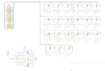
Yes, but I would believe that it is not ground referenced, because all supplies are floating (I could be wrong). It is possible that there are potential differences above 3KV between the individual supplies depending on the drivers position in the stack, But as long as there is sufficient clearence between the supplies there is no arcing, and I have not observed any arcing in the transformer either.

Here are the low-voltage power supply and control schematic.

lv-power.pngcontrol-1.png
 

there is a gap in your understanding, how do you level shift the gate drive signals to the input side of the gate drive chip? ( which is only good for 1200V )

this is not shown in your schematics ... nor are the IGBT's
 

there is a gap in your understanding

Yes there are several gaps, I can not disagree.

how do you level shift the gate drive signals to the input side of the gate drive chip? ( which is only good for 1200V )

The level shifting, and I only have this one place where I do any level shifting, is shown in the control schematic in post #23 it is a translation between 3.3V/15V and that is done by the MC14504B's. It's probably not what you mean, but that is what there is.

this is not shown in your schematics ... nor are the IGBT's

The IGBT's are shown in the schematic in #17. I had to split it up like that in KiCad in order to get each circuit on it's own PCB.
 

Not necessarily driver isolation failure, but may be functional failure resulting in inadvertent turn-on. Just a guess.

There are many ways to trace failure causee, e.g. disconnecting IGBTs, shorting GE terminals, measuring currents, etc.
 

It's been two months now for me just to make a couple of IGBT's behave somewhat orderly, and I still haven't been able to make anything stable above 2KV, so I'm putting this aside until further notice and I will have a re-think.
 

I think you are starting to understand the issue - you cannot have all ground referenced control to the gate drive chips - as soon as there is > 3kV across the gate drive chip it will fail - thus you need to use transformers to level shift the gate drive signal to the GD chips - as you have done for their local supply rail ...

- - - Updated - - -

there are other ways to switch a string of HV IGBT's or mosfets without using such chips - just by biasing the gates - likely in a thread on here ...
 

I think you are starting to understand the issue - you cannot have all ground referenced control to the gate drive chips - as soon as there is > 3kV across the gate drive chip it will fail - thus you need to use transformers to level shift the gate drive signal to the GD chips - as you have done for their local supply rail ...

Not only that, I find IGBT's are fragile, demanding and high maintenance - much like my ex-wife.

there are other ways to switch a string of HV IGBT's or mosfets without using such chips - just by biasing the gates - likely in a thread on here ...

Yes, but not in any thread here, i checked before positing. I was also looking at what is called self-powered gate drive, but from now on I will avoid mixing solid-state and HV, it's an ugly cocktail. I will be doing the switching industrial oldskool style, with hydrogen thyratrons.
 

When stacking devices there is a chance that one is "weaker"
than the rest and will leak enough that it doesn't stand off
its fair share of voltage; if the stack has no margin then the
rest may see > rec max, maybe > abs max voltage and break
down softly, with soft breakdown evolving into a hard fault.

Dynamic stacks have additional issues like the stray capacitance
and differing dV, hence dV/dt, leading to nonideal voltage
partitioning in-the-moment.

On RF switches I've seen designers add tuned capacitance
to keep the various switches in high stacks "in sync" and
standing off equal crest voltage.
 

Search: 5kV/200ns Pulsed Power Switch based on a SiC-JFET Super Cascode.
J. Biela, D. Aggeler, D. Bortis and J. W. Kolar
Power Electronic Systems Laboratory, ETH Zurich
Email: biela@lem.ee.ethz.ch

- - - Updated - - -

and read the pdf - shows SiC but mosfet or IGBT could be used ...

- - - Updated - - -

Also try and find some 8kV opto couplers and use these to convey the off on signals to the input of your gate driver chips ( both sides of the GD chip powered from your local isolated supply - ref to each emitter)

you then won't have > 3kV across your GD chips - it will be across the opto's - and things will work - try and use a ckt that maximises the speed of the opto ( e.g. common base with Schmidt trigger buffer ) and put small CM chokes ( a few turns on a bead ) on each opto input ( i.e. LED ) to limit CM dv/dt induced signals in the driver control...
 

Status
Not open for further replies.

Part and Inventory Search

Welcome to EDABoard.com

Sponsor

Back
Top