Continue to Site

Welcome to EDAboard.com

Welcome to our site! EDAboard.com is an international Electronics Discussion Forum focused on EDA software, circuits, schematics, books, theory, papers, asic, pld, 8051, DSP, Network, RF, Analog Design, PCB, Service Manuals... and a whole lot more! To participate you need to register. Registration is free. Click here to register now.

[SOLVED] Different ways of presenting a circuit

Status
Not open for further replies.

TotalNoob

Newbie level 4
Joined
Jul 4, 2019
Messages
6
Helped
0
Reputation
0
Reaction score
0
Trophy points
1
Activity points
49
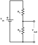
Hi, my problem is that i understand circuits like that:
circuit.png
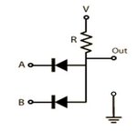
I can see where where the starting + and - of the battery would be, also i can see where the output is. It is really simple. But then, in school they showed me this
andJakimscudem.jpg
And they tell me that this works like AND gate. I dont understand how V is only one wire, and i have problems understanding how it works at all.
My question is: Does this way of presenting circuits have its own name?
Thank you for any potential help.
 

Didn't your teacher teach you? The AND gate is simple:
1) If both A and B inputs are not connected to anything or are both a logic high, then the diodes do not conduct so the resistor to the power supply causes the output to he high. Both A and B must be a logic high for the output to be high.
2) If one or both inputs A and B are at a logic low then it (they) conduct(s) causing the output to be low.
 

Re: Different ways of presenting a circuit

"Didn't your teacher teach you?" well i would not ask this question on a forum if he did.

And also, i dont understand what it mean to connect something to A. To my understanding you need 2 points, so that current can flow from one to the other, thats what my post is about.
 

I think the confusion is about where the source of voltage is. You have to imagine the point marked 'V' is the positive side of a battery and the ground symbol is the negative side of the battery, then it makes sense.

In the gate representation, it demonstrates what happens in a logic circuit, it actually is a working gate although it wouldn't work fast enough for computing. If 'A' or 'B' are at high logic level, which is assumed to be the same as supply voltage 'V', the diodes do not conduct so no current flows through the resistor, no voltage is dropped across it so the output is high. If either of 'A' or 'B' or both of them is taken to logic low (assumed to be ground voltage or 0V) current flows through the diode or diodes and through the resistor so it drops the voltage to a low level. Think of the diodes as being like R2 in your first schematic except that instead of them having a resistance they just hold the voltage at a low level, regardless of the current through R1.

Brian.
 

Thank you for your answer, it really helps. But now i have just one more question.
This is from your reply
"...the diodes do not conduct so no current flows through the resistor, no voltage is dropped across it so the output is high..."
I dont understand this part, if nothing flows through the resistor how is the "out" wire high?
 

Ohms law: V = I X R

If I is zero, meaning no current flows, then regardless of the value of R, V must also be zero. Remember this is the voltage dropped in R, so it will have the same voltage at both ends if I is zero.

In real life there will be a tiny amount of leakage through the diodes and some current will flow into whatever is connected to the output point but the voltage should be large enough to be recognized as logic high ('1') and when 'A' or 'B' or both are connected to a logic low level it should drop enough to be recognized as a logic low ('0').

Brian.
 
The hardest parst for me was the last thing you explained to me. But now it seems logical. Because i know the voltage drop can be calculated using the Ohms Law V=I*R and since I=0 then voltage drop is 0 so Out is still 5 v.
 

Hi

About the schematics:
The one shows
* a battery
* no GND node

The other just shows:
* A, B, V, OUT and a GND symbol.

In this case when one talks about "V" or "V voltage" ... without any other information, one expects the voltage is referenced to GND.

An example: Let´s say V = 5V, A = 4.5V, B = 0.5V ...
* then "V = 5V" means "V referenced to GND = 5V"
* the same is with A and B.
* if you want to say it the more exact, but also more complicated way, then you may say "A to GND voltage" or "A-GND voltage".

* but in case you don´t want to refer to GND you may say "A-B voltage", which means "Voltage_A_referenced_to_GND minus Voltage_B_referenced_to_GND" which is: 4.5V - 0.5V = 4.0V

***
Indeed the "V" in your circuit can be misleading.
In your case it just names the node. But often it is used as abbreviation for "Volts". Thus try to avoid V as name.

In datasheets you often may find V_AB ... which means "Voltage of node A referenced to node B"
Like at MOSFETs: There is Gate = G, Source = S. .... and when they talk about V_GS the mean the voltage of Gate referenced to the voltage of Source.

Klaus
 
Status
Not open for further replies.

Similar threads

Part and Inventory Search

Welcome to EDABoard.com

Sponsor

Back
Top