KingDarius6288
Junior Member level 2
Hi everyone,
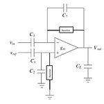
I have a question that might seem silly. I have an OTA that is going to be used in the attached configuration. The OTA ( an NMOS input single ended Folded Cascode, with a load capacitance of 20pF and open loop DC gain of 61dB) works perfect by itself, but when I connect the two C1 capacitors, the DC levels at the input of the OTA change significantly that affects the OTA open loop gain. In other words, the OTA is working with input common mode levels between 450-800mV, and Vin and Vref have the common mode level of 600mV normally. When I connect the two C1 capacitors, the DC level at the left side of C1 capacitors is 600mV but the DC level at the right is about 250mV. This eliminates OTA open loop gain. Does anyone know what is the reason and what should I do to solve it?
Thanks