Continue to Site

Welcome to EDAboard.com

Welcome to our site! EDAboard.com is an international Electronics Discussion Forum focused on EDA software, circuits, schematics, books, theory, papers, asic, pld, 8051, DSP, Network, RF, Analog Design, PCB, Service Manuals... and a whole lot more! To participate you need to register. Registration is free. Click here to register now.

LTC4020 component selection

Status
Not open for further replies.

Danie.

Newbie level 5
Joined
Jun 17, 2019
Messages
10
Helped
4
Reputation
8
Reaction score
4
Trophy points
3
Activity points
153
Hello,

i am about to design a buck boost Battery Charger with the LTC4020.

Design requirements:
- 10A charge current
- charge current adjustable
- 10V ... 48V input voltage
- different types of batterys (1s ... 12s LiPo, 6V, 12V, 24V lead accid -> adjustable output voltage range: 3V ... 53V)
- fully adjustable from a microcontroller

The first problem i have is to calculate the min. inductor value.
The datasheet is not really clear here and i am a bit confused about the use of IMAX and ILMAX and which one to use in the equations.

From the datasheet:
For step-down conversion, use the maximum expected operating voltage for VIN(MAX). If the expected VOUT
operating range (typically from VFBMIN = 2.125V to VFBMAX = 2.75V) includes VIN(MAX)/2, use that value for VOUT.
If the entire operating range is below VIN(MAX)/2, use the value corresponding to VFBMAX = 2.75V. If the entire operating
range is above VIN(MAX)/2, use the value correspondingto VFBMIN = 2.125V.
For step-up conversion, use the maximum output voltage (typically corresponding to pin VFBMAX = 2.75V) for VOUT(MAX).
If the expected VIN operating range includes VOUT(MAX)/2, use that value for VIN.
If the entire input operating range is below VOUT(MAX)/2, use the maximum operating voltage for VIN. If the entire input
operating range is above VOUT(MAX)/2, use the minimum input operating voltage for VIN.

Following this description, the worst cases are:

Buck: VinMax -> Vout = Vin/2 (48V -> 24V)
Lmin = (24V*(24V/48V)) / (120kHz*5A*10*) -> 2µH

Boost: VinMax -> VoutMax (48V -> 53V)
Lmin = (48V*(1-(48V/53V)) / (120kHz*11,45A*10A)) -> ~ 1,06µH


For me these values seems to be quite a lot to small!? Did i miss something here?
The Eval Board uses a 5,6µH Inductor.

Magnetics vendors typically specify inductors with maximum RMS and saturation current ratings.
Select an inductor that has a saturation current rating at or above 1.25 • IMAX, and an RMS rating above IMAX.
So i would use a 5,6µH inductor with an RMS current of >= 10A and a saturation of 10A*1,25 = 12,5A?
For me this seems to be completely wrong? :-o

Is this requirement possible at all?
If yes, how to adjust the voltage from an microcontroller?
Maybe a current sink DAC, wich adjusts the feedback node could do the job?
Current adjustment is done by sinking 0 to 50uA out from the RNG/SS and ILIM pin. So this should be quite easy.


Kind Regards
Danie
 

Hi,

The datasheet is not really clear here and i am a bit confused about the use of IMAX and ILMAX and which one to use in the equations.
In my eyes the datasheet is quite clear.
About IMAX the datasheet says:
where IMAX is the programmed inductor current limit.
= "dynamically adjustable via I_limit_pin
--> Read section "I_limit_pin"

About ILMAX datasheet says:
ILMAX is
the converter maximum inductor current as programmed by the two sense resistors.
= peak inductor current limit.
--> read section "RSENSEA, RSENSEB: DC/DC Converter Current Programming"

For me these values seems to be quite a lot to small!? Did i miss something here?
The Eval Board uses a 5,6µH Inductor.
No need to worry. (I ddidn't check your calculations)
You calculated 2uH minimum value. Now you need to choose an inductor that has at least 2uA worst case.
The inductor value (5,6uH) is the nominal value of the inductor. In reality this nominal value may be smaller due to production tolerance and inductor current..
Thus with 5.6uH you are on the safe side.

So i would use a 5,6µH inductor with an RMS current of >= 10A and a saturation of 10A*1,25 = 12,5A?
For me this seems to be completely wrong?
I assume you need to recalculate the values with the above given informations.
The values seem not to be "completely wrong".
My recommendation: don't go to the limit. Add some headroom.

If yes, how to adjust the voltage from an microcontroller?
Maybe a current sink DAC, wich adjusts the feedback node could do the job?
Basically yes.
You may have a look at this. Just use your DAC instead of PWM (if you like)
https://www.edaboard.com/showthread.php?377215-Design-of-PWM-controlled-SMPS-output-voltage

Klaus
 
Hello Klaus,

thank you for your reply!

What did
"...inductor maximum average current in the DC/DC converter inductor (ILMAX)"
average current here actually mean?
Is the average current the design current of 10A or is it the value calculated by:

For Step Down:
IL ~ Iin*(Vin/Vout)
Iin is not known!? - But the datasheet also says:
When the converter is stepping down, or operating in buck mode, the inductor current will be roughly
equivalent to the converter output current.
-> so here i could simply go with the 10A, right?


For Step Up:
IL ~ Iout*(Vout/Vin)
Which is greatest, if the Input is at VinMin and the output is on VoutMax. (Step Up 10V -> 53V)
So for IL ~ 10A*(53V/10V) ~ 53A.

So for RSENSEA = RSENSEB = 0,05/ILMax = 0,05/53A = ~0,943 milliohm
This is a realy unusual value, so i would go for 1 milliohm (->50A)?

So in general the inductor current limit:
- is equal to the desired output current in buck mode?
- needs to be calculated by the equiation of IL ~ Iout*(Vout/Vin) and lowered by servoing the ILIM-pin?

Later in the design i will lower the output current according to the input voltage. So input current is limited to about 5-10A in the worst case.
For know i first need to understand how to calculate the inductor value.


No need to worry. (I ddidn't check your calculations)
You calculated 2uH minimum value. Now you need to choose an inductor that has at least 2uA worst case.
The inductor value (5,6uH) is the nominal value of the inductor. In reality this nominal value may be smaller due to production tolerance and inductor current..
Thus with 5.6uH you are on the safe side.

I found an entry in the analog devices forum:
We had too low inductance. The formulas on page 23 have an extra 'Imax' term in the denominator, which shouldn't be there.
If you also were using that formula, you might have a too low inductance. Check it out. // Daniel

See post here: https://ez.analog.com/power/f/q-a/100595/ltc4020-unstable-operation/303106#303106
Could this be right?


For clarification:
In the equiation
LMIN = (VOUTx(1–VOUT/VIN(MAX) ) / (fO x deltaIMAX x IMAX))

What is deltaIMAX and what is IMAX?
According to the analog forum thread (see above) the IMAX denominator should be removed!?
This would yield to much higher min. inductor values!?

I am really confused right now.


Basically yes.
You may have a look at this. Just use your DAC instead of PWM (if you like)
Thank you for that link and schematic! This is what i was thinking about.
If i use the full output range from 3V to 53V output with 10 bit i get 50V/1024 ~ 49mV steps.
Is this enough accuarcy for a constant voltage charger?
Above 12 bits the DAC are getting quite expensive, so i would like to avoid this, if this is not really necessary!


Kind Regards
Danie
 

Hello Klaus,

after some time spend over the datasheet and some more calculations we had success with inductor selection.
Analog devices also confirmed our component selection.

We are currently about to finishing the schematics.
Last step is to implement the digital adjustment from uC. So i looked at your last post:

...
Basically yes.
You may have a look at this. Just use your DAC instead of PWM (if you like)
https://www.edaboard.com/showthread.php?377215-Design-of-PWM-controlled-SMPS-output-voltage

An MCP4728 I2C DAC is now used. (12 bits, 4 channel). 4 channel, because its much cheaper than devices with only two DAC channels.
This way its also possible to adjust VFBmin, VFBmax and the VIN_REG terminals.

But i am currently not sure about, what to do with the FBG-Pin. This pin provides a switched path to GNDS for the feedback resistor stings to lower current consumption, while the LTC4020 is in shutdown mode (SHDN = Low) or powered from battery.
When in shutdown the FBG pin is high impedance, which means the voltage on the DAC is equal to the voltage applied to the resistor strings.
So this would blow up my DAC, i guess?
The series resistance between the DAC outputs and the voltage dividers are 8k3.
Is this enough to protect the DAC from getting killed by overvoltage?


Another question regarding the SHDN-Pin:
Datasheet says:
When in shutdown, all charging functions are disabled and input supply current is reduced to 27.5µA.

So battery charging is disabled for sure. But is the DC/DC converter still running to power the system load? I guess no.

I would like to have a possibility to disconnect the battery (BGATE = High).
So when the DC/DC converter is running i could dynamically adjust the converter output voltage by measuring voltage with an ADC and servo the DAC output voltage until a desired output voltage is reached.

A way could be to pull down the RNG/SS pin to GNDS. But i am not sure if this would completely cut of the battery (BGATE = High)
Datasheet is not really clear here:
... RNG/SS voltage can also be manipulated using an active device, such as employing a pull-down transistor to disable charge current or to dynamically servo maximum charging current. Because this pin is internally pulled to ground during fault conditions, active devices with low impedance pull up capability cannot be used.

Does this mean, that pulling this pin to GNDS would completely disable the battery fet?
Currently i have a 20k digital potentiometer (AD5274) connected to the RNG/SS pin to adjust battery charge current from software.
This device has a maximum wiper resistance of 70 ohms. So setting DAC code zero should apply a voltage of about 70R*50e-6 = 3,5mV.
So maybe setting the DAC to zero could act as battery disconnect "switch"?


Thank you very much!

Kind Regards
Danie
 

Your Vin is 10 to 48v
Vout is 3 to 53v
Iout is up to 10A.

At 10Vin, your Iin is 53A max, so this will require paralled converters. I believe the LTC4020 has a transconductance error amplifier so its output can be joined to the output of the other LTC4020 error amp output.

I will look into your other qu's
 
  • Like
Reactions: Danie.

    Danie.

    Points: 2
    Helpful Answer Positive Rating
Forum EDA:
Your Vin is 10 to 48v
Vout is 3 to 53v
Iout is up to 10A.

At 10Vin, your Iin is 53A max, so this will require paralled converters. I believe the LTC4020 has a transconductance error amplifier so its output can be joined to the output of the other LTC4020 error amp output.

I will look into your other qu's

Hello treez,

its not necesarry for me to parallel converters, because the maximum charge current capability of 10A is only needed, if the input voltage is 24V or higher.
If the input voltage is to low, so that the inductor current would rise above 25A (limit set by sense resistor), the charge current is simply reduced by adjusting the voltage applied to the RNG/SS and Ilim pin with a digital potentiometer. (Vin is tracked by an ADC)

It would be great if you can take a look at the DAC and digital potentiometer related questions.
I will post some releated schematic parts later.

Thank you!

Kind regards
Danie
 

Hello,

here are the related schematic parts together with my questions:


First: voltage adjustment using DAC
voltageAdjustment.png

Questions:
1. Possible that way? I am not sure if i understand the battery stack voltage programming part correctly.
2. Is the series resistance of 8k3 (R306 ... R309) enough to protect the DAC (MCP4728) from overvoltage, while the FBG pin is open (SHDN = low)
3. What happens when the DC/DC converter is not operating? This should also result in overvoltage on the DAC pins?


Second: Battery voltage monitoring
adcMonitor.png

Questions:
1. To reduce current draw from battery i would like to attach the resistor strings to the FBG pin like in the first question.
Is the impedance high enough to protect the ADC? Or even to high to get enough precision?
MAX11613 datasheet says the input source impedance should be max. 1k5.
Maybe i can put a capacitor (100n?) to each ADC input to solve this issue? I do not really need high sample rates here!


Third: Current adjustment using digital potentiometer
currentAdjust.png

Questions:
1. Datasheet says about the RNG/SS Pin:
... RNG/SS voltage can also be manipulated using an active device, such as employing a pull-down transistor to disable charge current or to dynamically servo maximum charging current. Because this pin is internally pulled to ground during fault conditions, active devices with low impedance pull up capability cannot be used.
So does this mean by setting "BAT_FET_DISABLE" to high, the battery FET is completely disconnected? (BGATE pulled high)
Maybe the digital potentiometer at its lowest setting (max 70 ohms) could act in the same manner? - unfortunately datasheet did not specify a threshold voltage.


Fourth: Battery current measuring
BatCurrentMeasure.png
Questions:
1. Does this have high impact on the LTC4020 device operation? Datasheet specifies impedance of 100k.


Thank you very much!

Kind regards
Danie
 

Hi,

I didn't go through all your circuit, because this takes too much time for me.

But some thoughts:
1. Possible that way? I
this question is too general. What in detail do you want to ask?

I am not sure if i understand the battery stack voltage programming part correctly.
You try to do this linearely with huge dynamics. Isn't it easier/ more safe to use resistor strings and analog MUX to set for 1, 2, 3 ... cells? I assume you don't have 3.45 cells connected.

With your circuit, there are crossed out parts. What does that mean? Not decided yet, open, short circuit?

I recommend to focus at one part at a time.
Now I do this at V_FB node.
* Why 100nF from +BATT? I don't see it in the datasheet example circuit.
* You don't care about the FBG_open feature. I recommend to use an analog switch to your DAC to comply with it.
* the DAC output voltage is 0..2.048V...with 8k3 and 126k ( ratio of 15.2) you get a VBatt range of 2.048 x 15.2 = about 31V.
You want it that huge?

2. Is the series resistance of 8k3 (R306 ... R309) enough to protect the DAC (MCP4728) from overvoltage, while the FBG pin is open (SHDN = low)
For this you need to read the DAC datasheet about allowed pin current.

Anyway: The feature is used to protect against draining out the battery.... this is not valid anymore with your circuit.

Or even to high to get enough precision?
We don't know what precision you expect....

CSOut:
What waveform do you expect there?

In time I'm a bit busy, so I'll be back in more than 12h.

Klaus
 

Hello Klaus,

thank you for your reply!

You try to do this linearely with huge dynamics. Isn't it easier/ more safe to use resistor strings and analog MUX to set for 1, 2, 3 ... cells? I assume you don't have 3.45 cells connected.

I also thought this could be a much easier and cheaper solution. But the VFBmin/max pins also needs to be adjusted in the same way. So i would need that mux two times.
I would also like to support all chemistry's, the LTC4020 is able to charge. So i think it will be really complex to support all possible configurations.
All the resistors also should be 0.1% tolerance and for switching by the uC i would also need additional port expanders. So i came to the decision that its easier, cheaper and more flexible to use the single DAC instead.

With your circuit, there are crossed out parts. What does that mean? Not decided yet, open, short circuit?

I recommend to focus at one part at a time.
Now I do this at V_FB node.
* Why 100nF from +BATT? I don't see it in the datasheet example circuit.
* You don't care about the FBG_open feature. I recommend to use an analog switch to your DAC to comply with it.
* the DAC output voltage is 0..2.048V...with 8k3 and 126k ( ratio of 15.2) you get a VBatt range of 2.048 x 15.2 = about 31V.
You want it that huge?

Okay, so first lets focus on the DAC part only:
- crossed parts are not mounted.
- the 100nF are from the Demo Circuit 2134A.
- I also thought about using an analog switch IC but these also have to low voltage ratings (around 15V max). Maybe i could use a general N or P Fet? But how?

DAC output voltage is 3.3V (Vref=VDD)
So this would result in a range of about 50V. Lowest voltage is 3V, highest is 53V. So i am able to support the full range of the LTC4020.
Adjustment steps are ~12mV. (50V/4096 =12,2mV)


Regarding overvoltage protection of the DAC:
For this you need to read the DAC datasheet about allowed pin current.
Maximum pin current is +/-25mA. Worst case current (FBG open) is while DAC voltage is 0V. This will definitely result in a quite much lower current. (53V/126k+8k3 = ~0,4mA)
DAC impedance is typical in 1 ohms range. In power save mode of the DAC the impedance is selectable between 1k, 100k or 500k depending on the power down mode used.
If i only set the power down mode with 1k pulldown, i could not exceed the maximum voltage on the DAC pins? (1k*0,4mA = ~0,4V)
So there should be no problem with this configuration? (except current draw from battery)


We don't know what precision you expect....
Precision should be high enough to guarantee safe operation in all states.


CSOut: What waveform do you expect there?
In time I'm a bit busy, so I'll be back in more than 12h.

CSOUT is just an analog voltage representing the battery charge current -> VCSOUT = 0.25 + 20 • (VCSP – VCSN)
VCSP-VCSN is the voltage across the battery charge current sense resistor.

Danie
 

Hi,

DAC output voltage is 3.3V (Vref=VDD)
Makes no sense.
Before you talked about 0.1% resistors. This is initial accuracy ... and it has even less drift tgan thise 0.1%.
Then you talk about using VDD as VRef. VDD maybe with an initial accuracy of 5% and drift caused by input voltage, load, temperature and time....all this errors will be 1:1 transferred to the output...
Your system's overall precision will not be better than VDD precision.

Precision should be high enough to guarantee safe operation in all states.
Do you expect us to calculate the value(s)?

Klaus

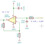
CSOUT is just an analog voltage representing the battery charge current -> VCSOUT = 0.25 + 20 • (VCSP – VCSN)
VCSP-VCSN is the voltage across the battery charge current sense resistor.
The battery current ... is it caused by a linear regulator, or ist it caused by a switching regulator...with high switching freqzency ... and high frequency currenr ripple?
 
  • Like
Reactions: Danie.

    Danie.

    Points: 2
    Helpful Answer Positive Rating
Hi Klaus,

sorry for the late reply - Project was on hold during vacation time...

Makes no sense.
Before you talked about 0.1% resistors. This is initial accuracy ... and it has even less drift tgan thise 0.1%.
Then you talk about using VDD as VRef. VDD maybe with an initial accuracy of 5% and drift caused by input voltage, load, temperature and time....all this errors will be 1:1 transferred to the output...
Your system's overall precision will not be better than VDD precision.

I missed that - you are right. That would result in terrible drifts...
So the analog part now has its own 5V regulator and the DAC is configured to use its internal reference voltage of 4.096V.
Here is the related schematic part:
DAC_VoltageAdjustment.png
I am currently not sure about the n-fets - Could this work? Same is implemented for the ADC inputs.

The battery current ... is it caused by a linear regulator, or ist it caused by a switching regulator...with high switching freqzency ... and high frequency currenr ripple?
Its caused by a switching regulator - My fault :laugh:
I assume that this signal should be a square wave? So a simple RC low pass filter should do the job?
Switching frequency is 250kHz. Could something like this work?
CSOUT_OP.png

Kind Regards
Danie
 

Hi,

Your current measurement:

First: standard signal flow at a schematic schould be from left to right.

The first Opamp (right side in your schematic) gets high frequency input. But the Opamp may be too slow to amplify it correctly, thus the output will be distorted and unreliable. The error will not be calculable.

To avoid this you should place an RC LPF in front to the Opamp.

Klaus
 

First: standard signal flow at a schematic schould be from left to right.
I know - but there was just not enough space left :bang:

The first Opamp (right side in your schematic) gets high frequency input. But the Opamp may be too slow to amplify it correctly, thus the output will be distorted and unreliable. The error will not be calculable.To avoid this you should place an RC LPF in front to the Opamp.

So this does actually mean, that the first opamp is useless?
Does this affect the current control loop of the LTC4020? According to the datasheet the CSOUT pin has an output impedance of 100k.
Current Sense Amplifier Output and Charge Current Monitor. Connect 100pF capacitor to ground. Pin output impedance is 100kΩ, so any loading for monitors must be high impedance.
That was the reason why i placed the buffer right after the CSOUT pin.
If i put the RC LPF in front of the Opamp i could also just simply build an active LPF (first order) with only one Opamp?
Like this:
CSOUT_OP_V1.png

Kind Regards
Danie
 

Hi,

If CSOUT output impedance really is 100k, then an external capacitor will reduce output bandwidth .....then I have to admit that an Opamp as buffer might work.

But a single Opamp circuit, like in your last picture, should work.

Klaus
 
  • Like
Reactions: Danie.

    Danie.

    Points: 2
    Helpful Answer Positive Rating
Status
Not open for further replies.

Part and Inventory Search

Welcome to EDABoard.com

Sponsor

Back
Top