prateek3790
Full Member level 2
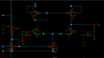
Hi All,
Can anyone share any document for designing the active load diff amp. I tried designing one with the following specs
VDD = 1.8v, GainBW = 5MHz, Cload = 10pf, ICMR+ = 1.6v, ICMR- = 0.8V, SLEW RATE = 5V/usec, Pdiss <0.3mw.
i started with getting the required tail current source. using slew rate info I_tail = 50uA.
i also calculated the vt and beta values for both pmos and nmos by connecting then in diode connected mos config and making w/l =1.
now from the icmr+ data got the voltage at the mid point(between diode connected pmos load and input nmos) so from there got the required vsd = vsg for pmos. and since the current will be I_tail/2 so calculated the required w/l for the pmoses.
now from the GBW data got the rquired gm data for the input nmos.again since the current itail/2. so got the required w/l.
from ICMR- got the required vdsat for the tail current mos and again calculated the w/l.
please tell whether this is a correct way or did i do some mistake.
i'm facing following issues.
- the tail current source is carrying half of the current even though i'm mirroring 50uA.
- unable to get the required GBW and gain.
so basically my circuit didn't work.Will really appreciate if you guys can tell whether the way i proceeded is wrong(i'm checking my calculations again).
If ny of you can share a basic document for the circuit it'll be of great help.
btw i kept the current mirror dimension same as the tail current even the vgs values are matching. both nmos(input are same) both pmos(active load ) are same.