Hawaslsh
Full Member level 3
- Joined
- Mar 13, 2015
- Messages
- 164
- Helped
- 5
- Reputation
- 10
- Reaction score
- 7
- Trophy points
- 1,298
- Location
- Washington DC, USA
- Activity points
- 3,422
Hello all,
I've recently had to migrate from ADS to Microwave office, and I'm trying to figure out some of the basics with the EM simulation tools. I've had success with microstrip lines, both 3D and 2.5 D simulators. However, when i try to model CPW lines, I begin to run into an issue. As the software suggests, I was able to model some CPW structures using the EMSight.
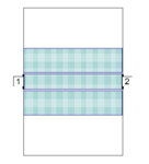
I created the simplest model possible. The stack up is one dielectric layer (not included the air) , one metal layer, and a copper ground plane. Using some dimensions from TxLine, i created a 50 Ohm line and the simulator had no issues. I created a circuit schematic to compare the EM results to an actual measured line, and a circuit model using the CPW closed form model in microwave office.
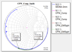
The simulated results don't match the loss of the measured line correctly, but I can be sure the EM simulation is giving me reasonable results. I run into a problem when I try and change the line geometry to a high impedance line. I changed nothing about the model setup, but i reduced the center line thickness to try and model a ~150 Ohm line, I begin to run into problems.
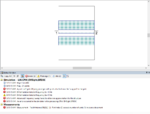
I've tried scouring the net for solutions to the errors i get (shown at the bottom of the figure above). I am having no luck. Any advice would be much appreciated.
Thanks in advance,
Sami
I've recently had to migrate from ADS to Microwave office, and I'm trying to figure out some of the basics with the EM simulation tools. I've had success with microstrip lines, both 3D and 2.5 D simulators. However, when i try to model CPW lines, I begin to run into an issue. As the software suggests, I was able to model some CPW structures using the EMSight.

I created the simplest model possible. The stack up is one dielectric layer (not included the air) , one metal layer, and a copper ground plane. Using some dimensions from TxLine, i created a 50 Ohm line and the simulator had no issues. I created a circuit schematic to compare the EM results to an actual measured line, and a circuit model using the CPW closed form model in microwave office.

The simulated results don't match the loss of the measured line correctly, but I can be sure the EM simulation is giving me reasonable results. I run into a problem when I try and change the line geometry to a high impedance line. I changed nothing about the model setup, but i reduced the center line thickness to try and model a ~150 Ohm line, I begin to run into problems.

I've tried scouring the net for solutions to the errors i get (shown at the bottom of the figure above). I am having no luck. Any advice would be much appreciated.
Thanks in advance,
Sami
