idijoeteque11
Newbie level 4
Hello all,
I am designing an isolated high voltage power supply with the aims of reducing the overall system size and weight, increasing power density. This is leading me to find converter topologies which are capable of operating at high frequencies efficiently. I have been studying the series resonant, parallel resonant, LCC and LLC converters for this task as they can absorb transformer non-idealities into the resonant tank design, meaning higher frequency operation can be achieved without parasitic effects. I have recently came across, however, a technique called the three-level DC/DC converter (Neutral point clamped, flying capacitor, diode clamped etc). Every paper I read on this states that it allows the MOSFET/IGBT switches to be operated at much higher frequencies with much more efficiency than standard 2 level designs. However, as of now, none of them offer why this is the case.
My ideas are as follows:
1) The voltage stresses on the devices are reduced, therefore the stress at a switching instant is reduced by half. However, this seems pointless if wide band-gap devices or soft-switching techniques are used.
2) the transformer is subject to a quasi-resonant square wave, removing the effects of operating a transformer at high frequency driven with a square wave voltage (due to harmonic content, etc).
And that's about as far as I can tell the benefits. However, I wish to use WBG devices and use some kind of soft-switching techniques, and my input voltage is only maximum 300V, so I'm unsure if the reduced switch stress is a massive plus either.
If anyone has any input, or any recommendation for other possible high frequency isolated, high output voltage DC/DC converter topologies that I could investigate (or general tips) then I would be very grateful for that.
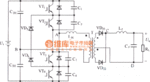
I have attached a standard DC/DC 3L converter image.
Thanks in advance,
")
I am designing an isolated high voltage power supply with the aims of reducing the overall system size and weight, increasing power density. This is leading me to find converter topologies which are capable of operating at high frequencies efficiently. I have been studying the series resonant, parallel resonant, LCC and LLC converters for this task as they can absorb transformer non-idealities into the resonant tank design, meaning higher frequency operation can be achieved without parasitic effects. I have recently came across, however, a technique called the three-level DC/DC converter (Neutral point clamped, flying capacitor, diode clamped etc). Every paper I read on this states that it allows the MOSFET/IGBT switches to be operated at much higher frequencies with much more efficiency than standard 2 level designs. However, as of now, none of them offer why this is the case.
My ideas are as follows:
1) The voltage stresses on the devices are reduced, therefore the stress at a switching instant is reduced by half. However, this seems pointless if wide band-gap devices or soft-switching techniques are used.
2) the transformer is subject to a quasi-resonant square wave, removing the effects of operating a transformer at high frequency driven with a square wave voltage (due to harmonic content, etc).
And that's about as far as I can tell the benefits. However, I wish to use WBG devices and use some kind of soft-switching techniques, and my input voltage is only maximum 300V, so I'm unsure if the reduced switch stress is a massive plus either.
If anyone has any input, or any recommendation for other possible high frequency isolated, high output voltage DC/DC converter topologies that I could investigate (or general tips) then I would be very grateful for that.
I have attached a standard DC/DC 3L converter image.
Thanks in advance,