Continue to Site

Welcome to EDAboard.com

Welcome to our site! EDAboard.com is an international Electronics Discussion Forum focused on EDA software, circuits, schematics, books, theory, papers, asic, pld, 8051, DSP, Network, RF, Analog Design, PCB, Service Manuals... and a whole lot more! To participate you need to register. Registration is free. Click here to register now.

OTA Closed Loop Test

Status
Not open for further replies.

KingDarius6288

Junior Member level 2
Joined
May 10, 2019
Messages
24
Helped
0
Reputation
0
Reaction score
0
Trophy points
1
Activity points
210
Hi all;

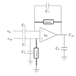
I have designed a two-stage OTA with Miller compensation. The first stage is Folded Cascode and the second one is a simple common source. The DC gain is 88dB and PM=35 deg. The load is a 10pF capacitor. I want to test it with capacitive feedback as below (attachment). The value of the resistor is very high and the C1 and C2 are in pF range. I have two questions:

1- Should the DC levels of Vin and Vout be equal? since the capacitive coupling f the input indicates that DC level of the input is zero, and the output DC level is not, I am somehow confused.

2- when I close the loop, voltage gain drops to negative dB values. can anyone suggest the reason and the solution?

Thank you in advance.
 

Attachments

  • OTA.png
    OTA.png
    30.9 KB · Views: 130

We can't discuss DC voltage levels without considering the OTA power supply. What are the input common mode and output voltage range?
Presuming sufficient power supply margin and zero OTA input current, Vout would be biased to zero, independent of Vin.

Circuit gain depends on C1/C2 ratio, and for low frequencies for the cut off frequency set by C2*R. Did you calculate it?
 
Thank you FvM. I have designed two OTAs with two different ranges. The first one has an input CM range of 0-0.2 and the second one has an input CM range of 0.4-0.7. Both of them have an output voltage range of 0.4-0.8. Do you see any problems with the mentioned ranges?

actually, the output that I get with capacitive feedback makes no sense. The gain is in -20dB range. I need a low cut off frequency of 10Hz but as I said the output ac response makes no sense and the gain is far below the C1/C2 value.
Do you have any suggestion to fix this?

Thanks
 

Thanks again FvM,

This might seem silly, but I could not your idea. so let me put my question this way:
1- If I design the OTA with fixed and equal DC levels for Vin+, Vin-, Vout, will it solve the problem?
2- I always thought that when the ICMR and the output range has a common range the OTA will work with feedback since feedback will fix the output DC value. (in my case the output (0.4-0.8) has a common range with the ICMR of (0.4-0.7)).

Thanks
 

I have designed two OTAs with two different ranges. The first one has an input CM range of 0-0.2 and the second one has an input CM range of 0.4-0.7. Both of them have an output voltage range of 0.4-0.8. Do you see any problems with the mentioned ranges?
None of both seem to be able to achieve correct DC bias with the given circuit, this might well explain the low AC gain.

The bias condition for this circuit is Vout = Vin- = Vin+, a DC voltage need to be applied to the input bias resistor, additionally you need a voltage divider or something similar for the CM range 0-0.2V.

- - - Updated - - -

Or design a different test circuit. It's easy to check the operation point of all transistors in simulation and see if it's appropriate.
 

Status
Not open for further replies.

Similar threads

Part and Inventory Search

Welcome to EDABoard.com

Sponsor

Back
Top