Welcome to our site! EDAboard.com is an international Electronics Discussion Forum focused on EDA software, circuits, schematics, books, theory, papers, asic, pld, 8051, DSP, Network, RF, Analog Design, PCB, Service Manuals... and a whole lot more! To participate you need to register. Registration is free. Click here to register now.
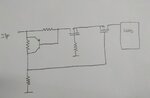
The left MOSFET is a low voltage drop polarity protection. It will be off if the input voltage is reversed.
When the current gets too high, the bipolar transistor will turn on and remove the gate voltage from the right MOSFET.
The MOSFETs are P-channel.
Sadly you didn't give more informatiin about current limit...
--> Just say you want it to be limit to 10mA nominal.
R1 .... is the "shunt" for current measurement.
Q1 .... should become conductive during current limit.
--> Q1 needs about 0.6V V_BE to become conductive. Now with 0.6V and 10mA you are able to calculate R1.
--> R2 is no needfed, as long as V_GS_max of Q3 is higher than the battery voltage.
--> R3 and R4 are not critical. They just need to drive the tiny gate current of Q3/Q2 (and the leakage current of Q1). Choose 100k down to 10k
--> Q1, Q2, Q3 need to widthstand battery voltage and max limiting current.
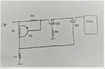
For my application, I want to limit max allowable current to 50mA. Upon that, the circuit should be protected.
From this, I have calculated R1 as 0.6V x 50mA => 30mOhms
R2 is no needed means. Then should I short the connections of Q1 collector and emitter? Kindly clarify.
R3 = 100K; R4 = 10K;
Q2 and Q3 => BSS84-7-F, MOSFET P-CH 50V 130MA SOT23-3.
...........
R2 is no needed means. Then should I short the connections of Q1 collector and emitter? Kindly clarify.
R3 = 100K; R4 = 10K;
Q2 and Q3 => BSS84-7-F, MOSFET P-CH 50V 130MA SOT23-3.
This site uses cookies to help personalise content, tailor your experience and to keep you logged in if you register.
By continuing to use this site, you are consenting to our use of cookies.