+ Post New Thread
Results 1 to 5 of 5
-
3rd June 2019, 03:22 #1
- Join Date
- Mar 2017
- Posts
- 58
- Helped
- 1 / 1
- Points
- 690
- Level
- 5
Op-amp and compensation
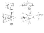
I have attached a figure that shows buffer in both non-inverting (a) and inverting configuration (b). Out of these two, which one is better if the op-amp has an offset.
In (c), (d), I am trying to do miller compensation with pole-zero cancellation. Which one of (c), (d) is better (especially when Cc has parastic caps that's proportional to Cc as shown in (e))?
-
Advertisement
-
3rd June 2019, 06:41 #2
Awards:
- Join Date
- Apr 2014
- Posts
- 16,056
- Helped
- 3635 / 3635
- Points
- 79,089
- Level
- 68
Re: Op-amp and compensation
Hi,
I have attached a figure that shows buffer in both non-inverting (a) and inverting configuration (b). Out of these two, which one is better if the op-amp has an offset.
Regarding output offset voltage..
* the noninverting circuit has benefits
Regarding stability:
* the inverting circuit has benefits
KlausPlease don´t contact me via PM, because there is no time to respond to them. No friend requests. Thank you.
-
Advertisement
-
3rd June 2019, 18:16 #3
- Join Date
- Nov 2013
- Posts
- 734
- Helped
- 199 / 199
- Points
- 4,973
- Level
- 16
Re: Op-amp and compensation
One point of Miller compensation is to transform a smaller capacitance to a bigger value and it will appear on the highest resistive value node, which is the OTA's output. It determines the dominat pole, you should add parasitics closer to that node, so I think (c) is better than (d).
Other thing, Cc is usually a MIM (Metal-Insulator-Metal) or MOM (Metal-Oxide-Metal) capacitor, where the parasitic capacitances at the pins are not the same regurarly in the model, so actually at one end of Cc you have x*Cc, on the other end y*Cc. These are coming from the MIM's and MOM's structure, and you should connect that terminal of Cc closer to the OTA's output which has the bigger parasitic capacitance, from last reason I mentioned above. I think this is logical, not sure.
Btw run a simulation with foundry models, and where the stability is better choose that arrangement."Try SCE to AUX." /John Aaron/
-
Advertisement
-
3rd June 2019, 20:00 #4
- Join Date
- Nov 2001
- Location
- US
- Posts
- 832
- Helped
- 264 / 264
- Points
- 9,718
- Level
- 23
Re: Op-amp and compensation
Regarding the offset: a) gains up the input referred offset by 1x, while b) gains it up by 2x.
As to the Miller compensation: whether that parasitic cap is at the OTA node or the output node - it will get lumped with the rest of hte caps with those nodes and you just have to live with it. More interesting is the effect of the Cc parasitic caps in the node between the Cc and the resistor - this node produces a 3rd pole in the loop and you'll have to see what the effect of parasitics is there.
-
21st July 2019, 15:52 #5
- Join Date
- May 2007
- Location
- India
- Posts
- 385
- Helped
- 107 / 107
- Points
- 5,544
- Level
- 17
Re: Op-amp and compensation
On the choice of R-C vs C-R
1. If the R is implemented with MOS, then it has to R-C (fig(d)) as you can bias the transistor correctly and have fixed-R over output swing
2. In most cases the dominant pole is at the first stage output, so I would prefer to keep the capacitor end that displays the larger parasitic cap to the first stage output (fig(c)) so as to not make my compensation problem worse. But if (d) is preferred due to (1), I would keep the max parasitic cap end to the output to avoid generating another pole as sutapanaki mentioned - this is if R*Cpar is not negligible.
On the offset, as sutapanaki said (b) will have 2x the offset compared to (a). On top of this, the offset of (a) will vary with the input swing whereas (b) will not
+ Post New Thread
Please login